In this topic, you study the Boost Regulator Circuit diagram, Waveforms, Modes of operation & theory.
The boost regulator produces a higher average output voltage than the dc source input voltage. Let us assume large filter capacitance C connected across the load so that output voltage remains almost constant. The Resistive load is considered.
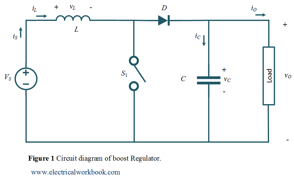
Circuit diagram
The working of a boost regulator is explained using the circuit diagram as shown in Figure 1. The regulation is normally achieved by PWM (Pulse Width Modulation) at a fixed frequency and using the switch ${S_1}$ shown in the circuit diagram can be a conventional thyristor i.e., SCR, a GTO thyristor, a power transistor, or a MOSFET.
Waveforms
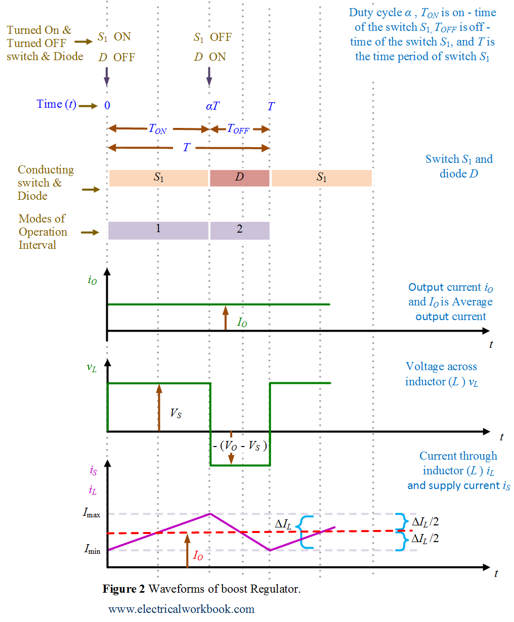
The typical waveforms in the converter are shown in Figure 2.
Modes of Operation Interval
The two modes in steady state operations are
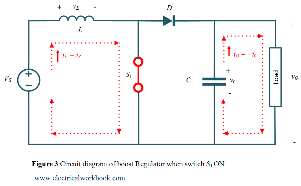
Mode of Operation Interval 1: –
The time interval is 0 ≤ t ≤ ${T_{ON}}$. The circuit diagram for Mode of Operation Interval 1 is shown in Figure 3 and the corresponding waveforms are shown in Figure 2. The switch ${S_1}$ is turned on, and the dc source directly connects to inductor L, the source (or input) current increases linearly and flows through the inductor L. The capacitor maintains the voltage ${v_O}$ across the load and hence supplies current ${i_O}$ to the load. The diode D gets reverse biased and behave as an open circuit. The inductor stores energy during this interval.
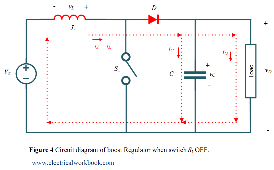
Mode of Operation Interval 2: –
The time interval is ${T_{ON}}$ ≤ t ≤ ${T_{OFF}}$. The circuit diagram for Mode of Operation Interval 2 is shown in Figure 4 and the corresponding waveforms are shown in Figure 2. The switch ${S_1}$ is turned OFF, the source (or input) current or the inductor current decreases linearly and flows through the Forward biased diode D, filter capacitor C, Resistive load. The inductor release energy during this interval.