In this topic, you study How to derive an expression for Peak to Peak ripple current for Boost Regulator.
The boost regulator produces a higher average output voltage than the dc source input voltage. Let us assume large filter capacitance C connected across the load so that output voltage remains almost constant. The Resistive load is considered.
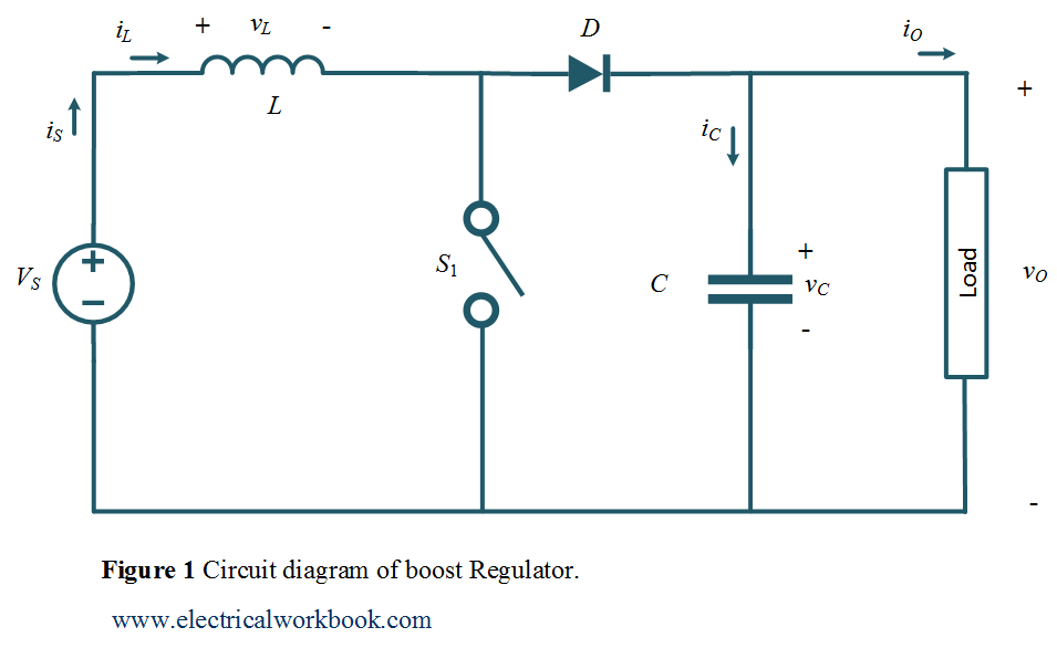
Circuit diagram
The working of a boost regulator is explained using the circuit diagram as shown in Figure 1. The switch ${S_1}$ shown in the circuit diagram can be a conventional thyristor i.e., SCR, a GTO thyristor, a power transistor, or a MOSFET.
Waveforms
The typical waveforms in the converter are shown in Figure 2.
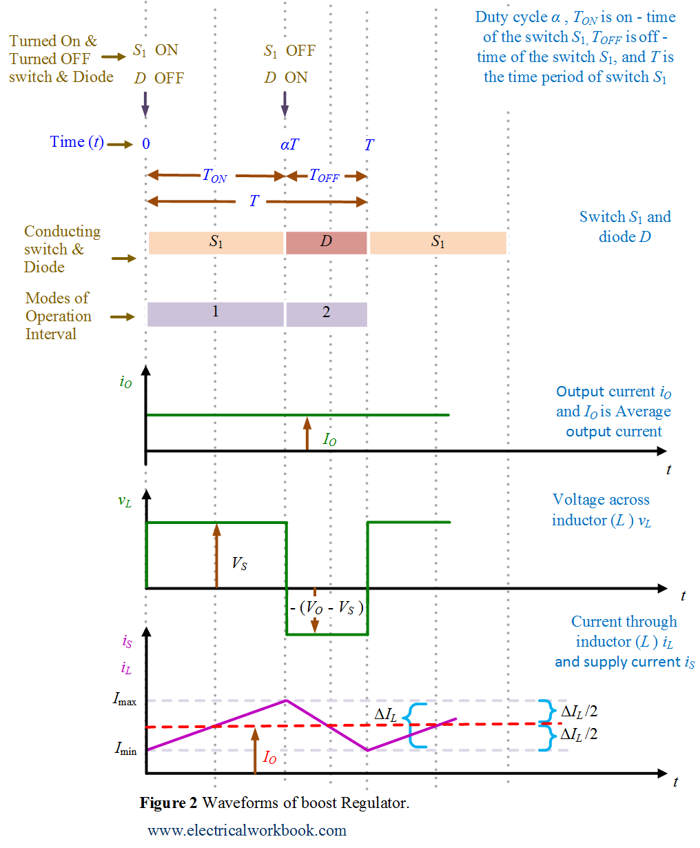
Mode of Operation Interval 1: –
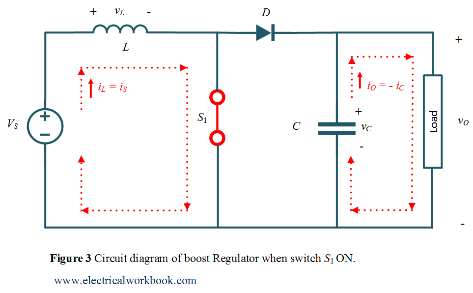
The time interval is 0 ≤ t ≤ ${T_{ON}}$. The switch ${S_1}$ is turned on. The circuit diagram for Mode of Operation Interval 1 is shown in Figure 3 and the corresponding waveforms are shown in Figure 2.
From the waveform of voltage across the inductor, as shown in Figure 2, the equation for the inductor voltage write as
\[{v_L} = {V_S} \hspace{1cm}….(1)\]
The general equation relates voltage across the inductor and current passes through it as
\[{v_L} = L\frac{{d{i_L}}}{{dt}} \hspace{1cm}….(2)\]
Put Equation 2 in Equation 1 gives
\[L\frac{{d{i_L}}}{{dt}} = {V_S}…(3)\]
The waveform for current passes through inductor L as shown in Figure 2, Integrate Equation 3 using the maximum and minimum value of inductor current gives
\[\int\limits_{{I_{\min }}}^{{I_{\max }}} d {i_L} = \frac{{{V_s}}}{L}\int\limits_0^{{T_{ON}}} d t\]
or
\[{I_{\max }} – {I_{\min }}\hspace{0.1cm} =\hspace{0.1cm} \frac{{{V_S}}}{L}.{T_{ON}} \hspace{1cm}….(4)\]
Here $\Delta {I_L} = {\text{ }}{I_{\max }}\hspace{0.1cm} – {I_{\min }}$ is the peak to peak ripple current of inductor L and hence Equation 4 can be write as
\[\Delta {I_L} = \frac{{{V_S}}}{L}.{T_{ON}} \hspace{1cm}….(5)\]
Also
\[{T_{ON}} = \alpha T = \frac{\alpha }{f} \hspace{1cm}….(6)\]
Using Equation 5 and Equation 6 gives
\[\Delta {I_L} = \frac{{{V_S}}}{L}.\frac{\alpha }{f} \hspace{1cm}….(7)\]
Equation 7 describes the peak to peak ripple current of inductor L in boost converter.