In this topic, you study How to derive an expression for Peak to Peak Ripple voltage of the capacitor for Boost Regulator.
The boost regulator produces a higher average output voltage than the dc source input voltage. Let us assume large filter capacitance C connected across the load so that output voltage remains almost constant. The Resistive load is considered.
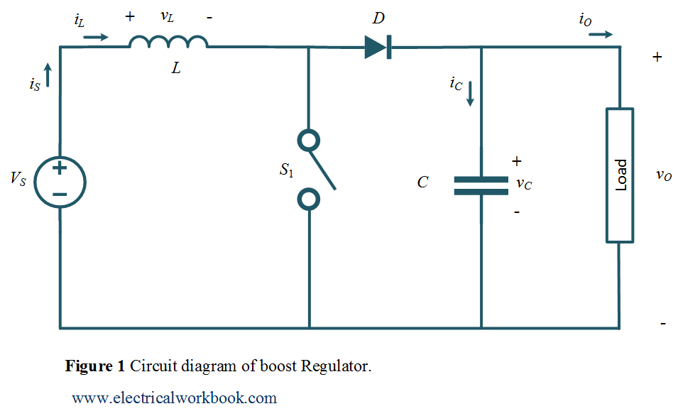
Circuit diagram
The working of a boost regulator is explained using the circuit diagram as shown in Figure 1. The switch ${S_1}$ shown in the circuit diagram can be a conventional thyristor i.e., SCR, a GTO thyristor, a power transistor, or a MOSFET.
Waveforms
The typical waveforms in the converter are shown in Figure 2.
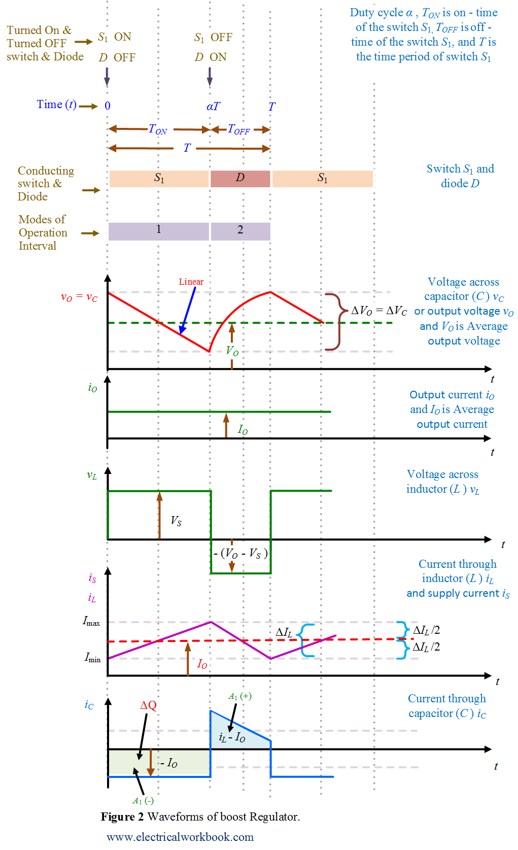
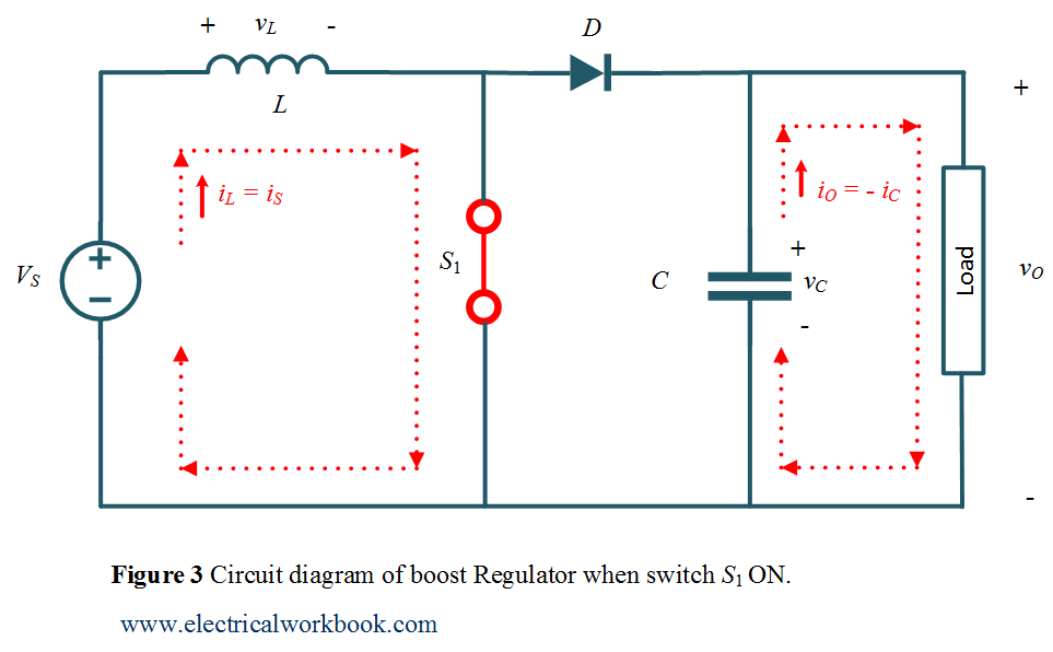
Mode of Operation Interval 1: –
The time interval is 0 ≤ t ≤ ${T_{ON}}$. The switch ${S_1}$ is turned on. The circuit diagram for Mode of Operation Interval 1 is shown in Figure 3 and the corresponding waveforms are shown in Figure 2.
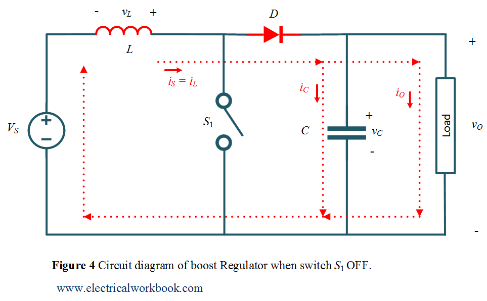
Mode of Operation Interval 2: –
The time interval is ${T_{ON}}$ ≤ t ≤ ${T_{OFF}}$. The circuit diagram for Mode of Operation Interval 2 is shown in Figure 4 and the corresponding waveforms are shown in Figure 2.
As shown in Figure 2, the area of rectangle ${A_1}$( – ) representing charge $\Delta Q$ in the waveform of capacitor current as shown in Figure 2, write as
\[\Delta Q = {I_O}\hspace{0.1cm}{T_{ON}}…..(1)\]
The change in voltage $\Delta {V_O}$ across the capacitor is associated with change in charge $\Delta Q$ by the relation
\[\Delta {V_O} = \Delta {V_C} = \frac{{\Delta Q}}{C}….(2)\]
Using Equation 1 and Equation 2 gives
\[\Delta {V_O} = \Delta {V_C} = \frac{{\Delta Q}}{C} = \frac{{{I_O}\hspace{0.1cm}{T_{ON}}}}{C}…(3)\]
The turn – on time ${T_{ON}}$ equation in terms of chopping frequency $f$ and duty cycle $\alpha$ as
\[{T_{ON}} = \frac{\alpha }{f}….(4)\]
Using Equation 3 and Equation 4 gives
\[\Delta {V_O} = \Delta {V_C} = \frac{{\Delta Q}}{C} = \frac{{\alpha\hspace{0.1cm}{I_O}}}{{Cf}}….(5)\]
Equation 5 describes the Peak to Peak Ripple Voltage of Capacitor in boost converter.