In this topic, you study Single Phase Full Bridge Inverter – Circuit Diagram, Working & Waveforms.
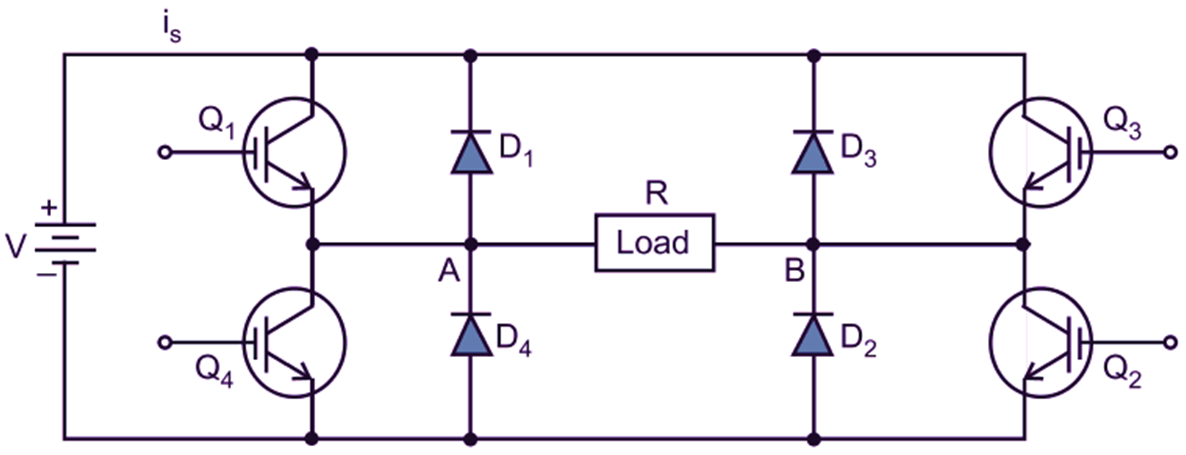
Fig. 1: Single Phase Full Bridge Inverter
The above Fig. 1 shows single phase bridge inverter with resistive load. The arrangement of the inverter consists of four transistor, (MOSFET or IGBT).To obtain an ac waveform at the output, the transistors are turned ON and OFF in pairs of Q1, Q2 and Q3, Q4. Thus to obtain a positive voltage (+V) across the load, the transistors Q1 and Q2 are turned ON (kept conducting) simultaneously, whereas to obtain a negative voltage (-V) at the output i.e. across the load, the transistors Q1 and Q2 are need to be turned ON. The diode D1, D2, D3, and D4 are acting as feedback elements as the energy is feedback to the source through them when the load is inductive in nature. The waveform of the single phase bridge inverter with resistive load is shown in the following Fig. 2.
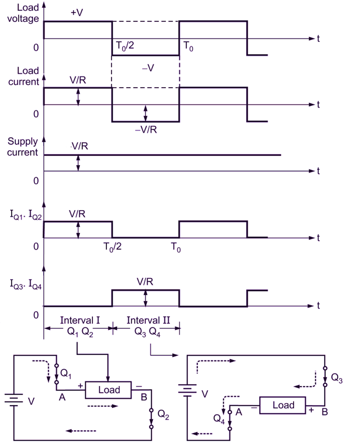
Fig. 2: Voltage and current waveforms with resistive load
Working of Single Phase Full Bridge Inverter
The working of the single phase bridge inverter with resistive load is explained in the following time intervals (modes):
Interval 1 (0 – T0/2) [Mode -1]:
During this interval, the transistors Q1 and Q2 are kept conducting simultaneously. Thus the load voltage appeared across the resistive load is +V volts and the direction (flow) of current is from A to B. The transistors act as closed switch when they are conducting. The equivalent circuit of Mode-I is shown in following Fig. 3.
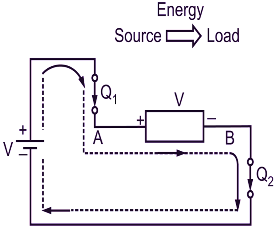
Fig. 33: Mode I
Interval 1 (T0/2 – T0) [Mode -2]:
During this time interval, the transistor Q3 and Q4 are turned ON at time, t = T0/2 while Q1 and Q2 are turned OFF at the same time (Fig. 4). The load voltage appeared the resistive load is -V volts and the direction (flow) of current isfrom B to A. Due to the resistive load the energy is not stored feedback diodes do not come into picture here.
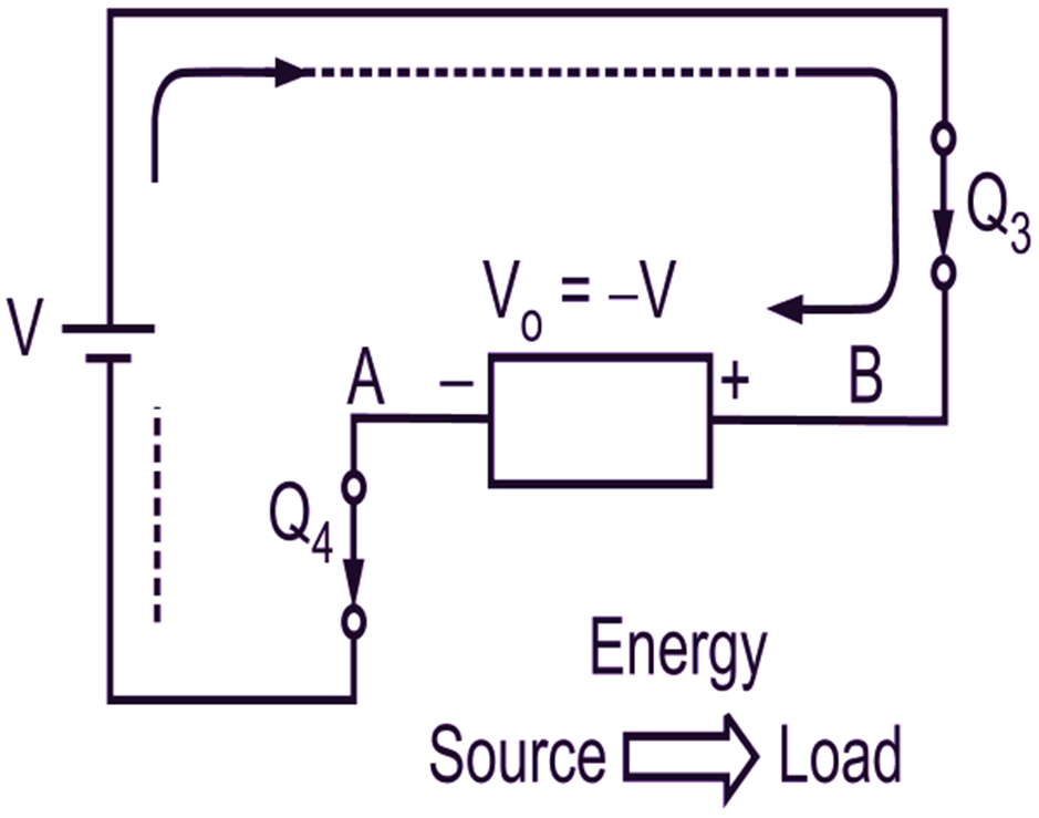
Fig. 4: Mode Il equivalent
Note
The load current and load voltage are in phase to each other. The conduction period of the transistors is 180°.
Maximum value of current through each transistor is,
\[{{\text{I}}_{\text{max}}}=\frac{\text{V}}{\text{R}}\]
Average value of current through each transistor is,
\[{{\text{I}}_{\text{avg}}}=\frac{\text{V}}{\text{2R}}\]
The maximum value of forward voltage across transistor is,
\[{{\text{V}}_{\text{max}}}=\text{V}\]