In this topic, you study Single Phase Half Bridge Inverter – Circuit Diagram, Working & Waveforms.
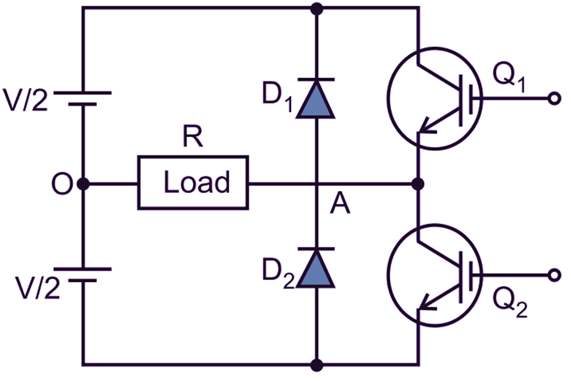
Fig. 1: Single Phase Half Bridge Inverter
The above Fig. 1 shows half bridge inverter using two transistors (MOSFET or IGBT). The diodes are used to protect the IGBT from blocking negative voltage. The diodes allow free-wheeling operation in case of inductive load. When only two switching devices are used for converting DC to AC then the configuration is known as half bridge inverter.
Working of Single Phase Half Bridge Inverter
The working of the half bridge inverter is as follows :
The transistor (MOSFET or IGBT) Q1 is turned ON for a time To/2 which makes the V/2 voltage appear across the load, resistance ‘R’. The value of output voltage (Vo) is given by
\[{{\text{V}}_{\text{o}}}=\frac{\text{V}}{2}\]
Similarly, when transistor Q2 is turned ON at the instant To/2 until time To, by turning OFF Q1 then – V/2 voltage appears across the load Resistance ‘R’. The waveforms are shown in Fig. 2. The amount of current flowing through the load is given by,
\[\text{Load current}=\frac{\text{V/2}}{\text{R}}=\frac{\text{V}}{\text{2R}}\]
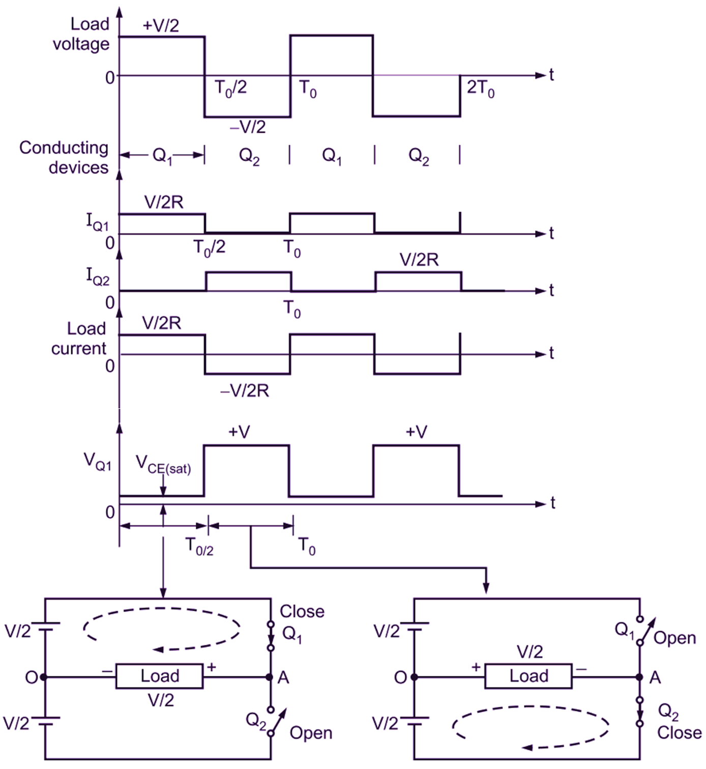
Fig. 2: Load voltage and current waveforms with resistive load for half bridge inverter