In this topic, you study Zener Breakdown – Definition & Theory.
When the PN junction is heavily doped, the depletion layer is narrow. When reverse voltage is increased, the electric field at the junction also increases. Due to increase in electric field at the junction, it breaks the covalent bond from the crystal structure. As a result of this, large number of minority carriers are generated. The minority charged carriers cross the junction because of narrow depletion layer. A large current flows through the junction due to minority carrier and the mechanism is called zener breakdown. The comparison of Zener breakdown between Ge and Si semiconductor diodes with respect to I–V curve shown in Figure 1.
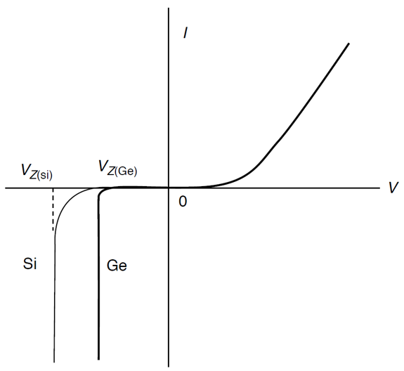
Fig. 1: Zener Breakdown on I–V curve.