In this topic, you study the Buck-Boost Regulator Circuit diagram, Waveforms, Modes of operation & theory.
The buck-boost regulator can produce an average output voltage less than or greater than the dc source input voltage. Let us assume large filter capacitance C connected across the load so that output voltage remains almost constant. The Resistive load is considered.
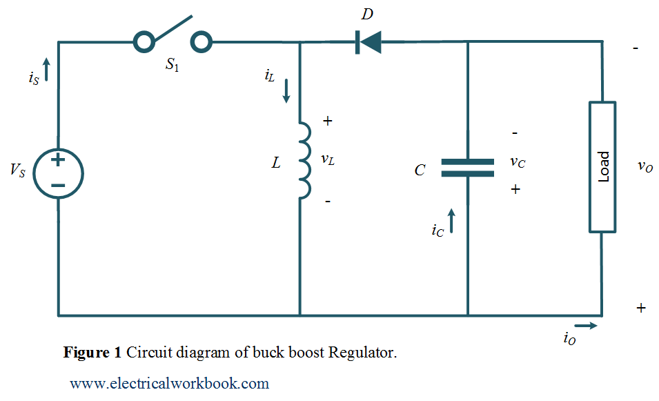
Circuit diagram
The working of a buck-boost regulator is explained using the circuit diagram as shown in Figure 1. The regulation is normally achieved by PWM (Pulse Width Modulation) at a fixed frequency and using the switch ${S_1}$ shown in the circuit diagram can be a conventional thyristor i.e., SCR, a GTO thyristor, a power transistor, or a MOSFET.
Waveforms
The typical waveforms in the converter are shown in Figure 2.
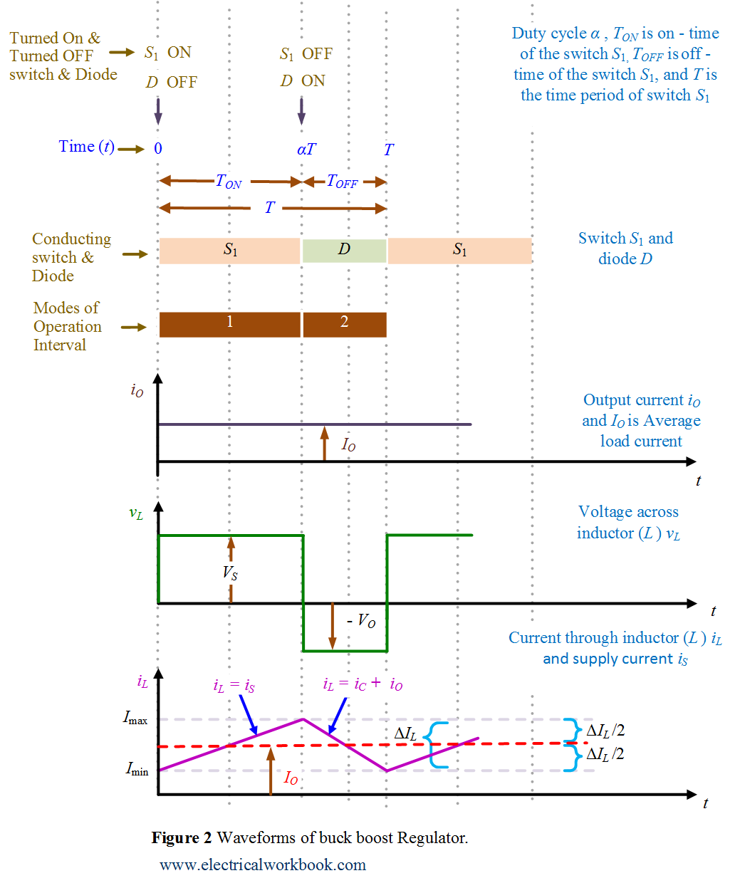
Modes of Operation Interval
The two modes in steady state operations are
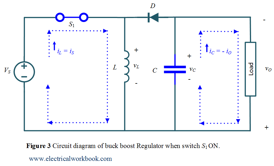
Mode of Operation Interval 1: –
The time interval is 0 ≤ t ≤ ${T_{ON}}$. The circuit diagram for Mode of Operation Interval 1 is shown in Figure 3 and the corresponding waveforms are shown in Figure 2. The switch ${S_1}$ is turned on, and the dc source directly connects to inductor L, the source (or input) current increases linearly and flows through the inductor L. The capacitor maintains the voltage ${v_O}$ across the load and hence supplies current ${i_O}$ to the load. The diode D gets reverse biased and behave as an open circuit. The inductor stores energy during this interval.
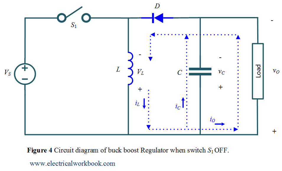
Mode of Operation Interval 2: –
The time interval is ${T_{ON}}$ ≤ t ≤ ${T_{OFF}}$. The circuit diagram for Mode of Operation Interval 2 is shown in Figure 4 and the corresponding waveforms are shown in Figure 2. The switch ${S_1}$ is turned OFF, the inductor current decreases linearly and flows through the Forward biased diode D, filter capacitor C, Resistive load. The inductor release energy during this interval.