In this topic, you study How to derive an expression of Average Output voltage and Duty Cycle for Buck Regulator.
The buck regulator produces a lower average output voltage than the dc source input voltage. Let us assume large filter capacitance C connected across the load so that output voltage remains almost constant. The Resistive load is considered.
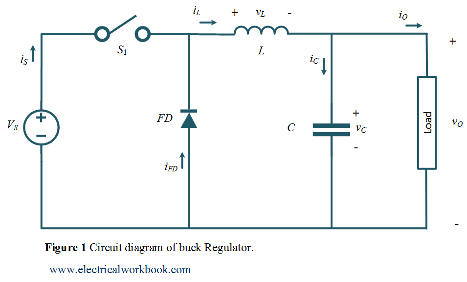
Circuit diagram
The working of a buck regulator is explained using the circuit diagram as shown in Figure 1. The switch ${S_1}$ shown in the circuit diagram can be a conventional thyristor i.e., SCR, a GTO thyristor, a power transistor, or a MOSFET.
Waveforms
The typical waveforms in the converter are shown in Figure 2.
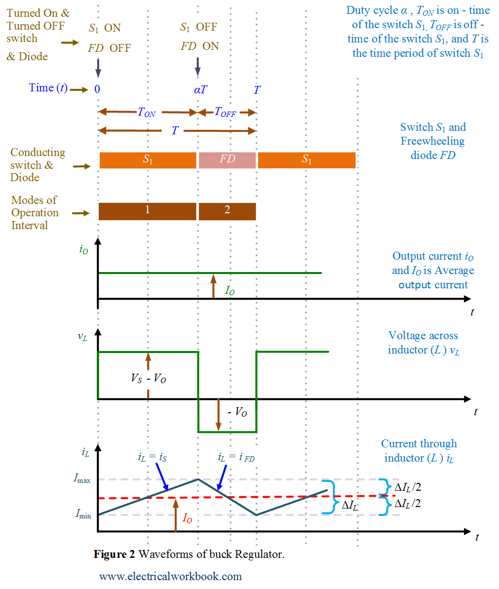
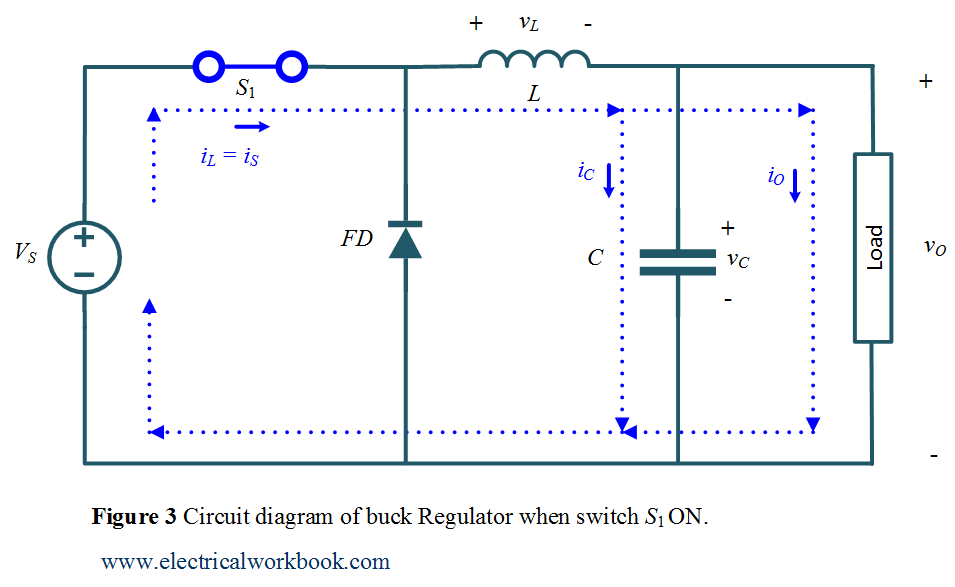
Mode of Operation Interval 1: –
The time interval is 0 ≤ t ≤ ${T_{ON}}$. The switch ${S_1}$ is turned on. The circuit diagram for Mode of Operation Interval 1 is shown in Figure 3 and the corresponding waveforms are shown in Figure 2.
Mode of Operation Interval 2: –
The time interval is ${T_{ON}}$ ≤ t ≤ ${T_{OFF}}$. The circuit diagram for Mode of Operation Interval 2 is shown in Figure 4 and the corresponding waveforms are shown in Figure 2.
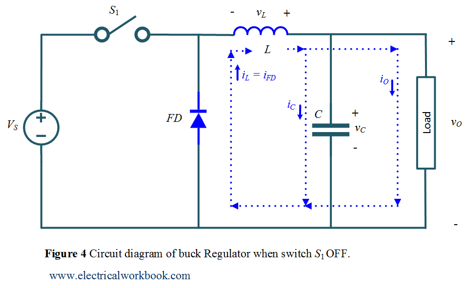
The current passes through the capacitor as shown in Figure 4 can be find using KCL,
\[{i_C} = {i_L}\hspace{0.1cm} – \hspace{0.1cm}{i_O}\]
From the inductor voltage waveform, as shown in Figure 2, the equation for inductor voltage write as
\[{v_L} =\hspace{0.1cm} – \hspace{0.1cm}{V_O}\]
According to Faraday’s Law, the inductor volt-second product over a period T of steady-state operation is zero.
\[{({v_L})_{avg}} = 0\]
So apply Faraday’s Law, using the inductor voltage waveform, as shown in Figure 2, the inductor volt-second product over a period T equation write as
\[({V_S}\hspace{0.1cm} – \hspace{0.1cm}{V_O})\hspace{0.1cm}{T_{ON}}\hspace{0.1cm} – {V_O}\hspace{0.1cm}{T_{OFF}} = 0\]
In simplified form as
\[{V_S}\hspace{0.1cm}{T_{ON}}\hspace{0.1cm} =\hspace{0.1cm} {V_O}\hspace{0.1cm}T\]
\[{V_O}\hspace{0.1cm} =\hspace{0.1cm} \alpha \hspace{0.1cm}{V_S}….(1)\]
where,
$\alpha$ = ${T_{ON}}\hspace{0.1cm}/\hspace{0.1cm}T$ and $\alpha$ is the duty cycle of the chopper.
Equation 1 describes the relationship between input dc source voltage and average output voltage in a buck converter.