In this topic, you study Full Wave Bridge Rectifier – Circuit Diagram, Working & Waveforms.
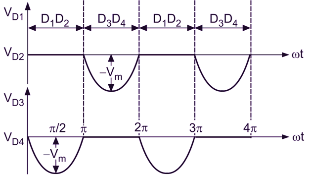
Fig. 1 shows a full wave bridge rectifier and its waveforms. When a is positive w.r.t. b, diodes D1 and D2 conduct. The output voltage is Vab. When b is positive w.r.t. a, diodes D3 and D4 conduct and output voltage is Vba.
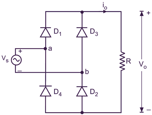
(a) Circuit Diagram
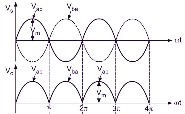
(b) Waveforms
Average output voltage
The average output voltage will be
\[{{\text{V}}_{\text{o}}}=\frac{2{{\text{V}}_{\text{m}}}}{\text{ }\!\!\pi\!\!\text{ }}\]