List of Components Needed for making PCB (Printed Circuit Board)
- Circuit diagram
- Components to be mounted
- Tracing paper and sketch pen
- Piece of thermocole
- Copper clad board and carbon paper
- Hacksaw
- File
- Emery paper
- Hard pencil
- Hand drill machines
- Drill bits (1/32)”, (l/8)”
- Drawing brush –
- White paint
- Razor
- Tray or dish
- Ferric chloride as etchant
- Hydrochloric acid as activator
- Turpentine oil.
Steps to make PCB
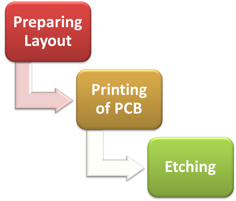
Preparing Layout
With the circuit diagram and all the components in hand, draw a complete layout plan on a tracing paper in the same way as an assembled PCB should look like. For this fix the tracing paper on a piece of thermocole and mount the components on the thermocole through the tracing paper. Show position of the components on the tracing paper showing symbol, and then mark the connecting wire (track) with the help of a sketch pen. Now remove components from the thermocole and give a finishing touch to the markings in such a way that all the connecting wires are shown in equal width with their terminals rounded oIE Case should be taken regarding location, shape and size of the components. Avoid overcrowding utilize the available space fully. Keep the supply line on one side and ground line on the other side.
Printing of PCB
The drawing so prepared is to be transferred onto the copper clad laminate. Keep in mind that the components are to be inserted from under side (non-clad side) of the board. for this proceed as follows:
- Take a PCB laminate sheet and cut a piece of required size by using a hacksaw. Now file the edges of the board carefully.
- Put the board on a table keeping copper side on the top. Clean the surface from dust, dirt, grease, oil, etc., using an emery paper.
- Now put a carbon paper on the board with its side lacing copper surface. Over it. put the drawing with its marked side facing the carbon paper and other side on the top. Since the tracing paper is transparent, you can now transfer a carbon print of the drawing (layout) over the copper surface of the board by rolling a hard pencil over the drawing on the transparent side.
- When a carbon print has been obtained on the board, drill holes in the board at required places using a hand drill machine. A bit 1/32” may be used for components’ leads and 1/8” bit for fastening screws. Sec that no part of the carbon print is erased or wiped out.
- Now paint the connecting lines (track) with the help of a drawing brush and white paint and allow the board to dry in the open. After the paint has dried, observe the board carefully. Make required touching for any missing connections. Any excess paint should be scratched off with the edge of a razor.
Etching
For etching (removing) copper from unwanted part of the board, proceed as follows: Remember copper is needed on the track and other circuitry (connections) required for the operation of the circuit. All the other copper from the surface of the board is to be removed or etched off:
- In a dish or tray, take fresh water and mix a few tea spoons of Ferric chloride (or cupric chloride). Now add few drops of Hydrochloric acid in the solution. The Hydrochloric acid is used as a catalyst (activator) to expedite the etching process. How keep the board dipped completely in this solution. Keep it infor about 15 – 25 min. The solution should be regularly stirred. The stirring also increases the etching speed and reduces the etching time.
- Observe the change of colour of the naked copper surface of the board. The copper except for the painted portion of the board will be completely dissolved in the solution. This can be seen by change of colour of the board as well as of the solution.
- Wash the board in running tap water.
- After the PCB has been thoroughly washed in water remove the paint by a soft piece of cloth dipped in a thinner or turpentine oil.
Finishing
After the above processes are carried out, the components can be assembled (mounted) on the board by soldering. A solder mask can also be provided prior to varnish for protection. The PCB in now ready for use, see Figure 1.
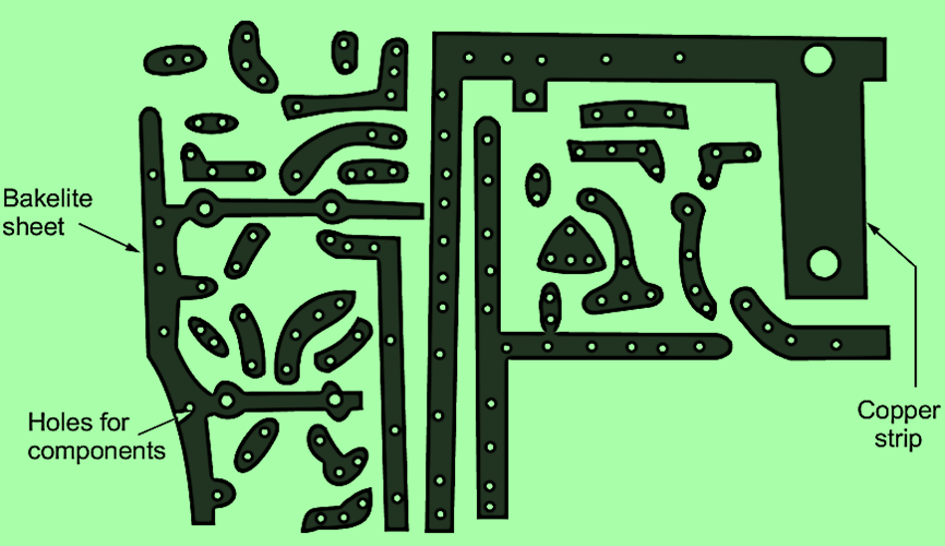
Fig. 1: PCB