A Printed Circuit Board (PCB) consists of a sheet of an insulating material. Small holes are provided on this sheet for accommodating different components of the circuit to be assembled. The components are automatically connected with each other through copper strips embedded within the sheet (Fig. 1).
Although each circuit has its own PCB, the method of manufacturing is more or less the same. First of all an insulating sheet of proper size is taken. The whole sheet is covered with copper foil. On this foil the circuit lines are drawn and covered with an enamel layer. After the enamel paint is dried up. the sheet is dipped into the solution of Ferric Chloride (Fe2Cl3) with few drops of Hydrocliloric acid (HCI). The copper (except the painted portion) is dissolved in the solution. Later on, this paint is cleaned off by petrol, etc. On this copper strip (track), holes are now drilled to accommodate components. Though each circuit has its own PCB, same PCB can be used for different circuits with slight modifications. But generally this is not done and a separate PCB is prepared for individual circuit.
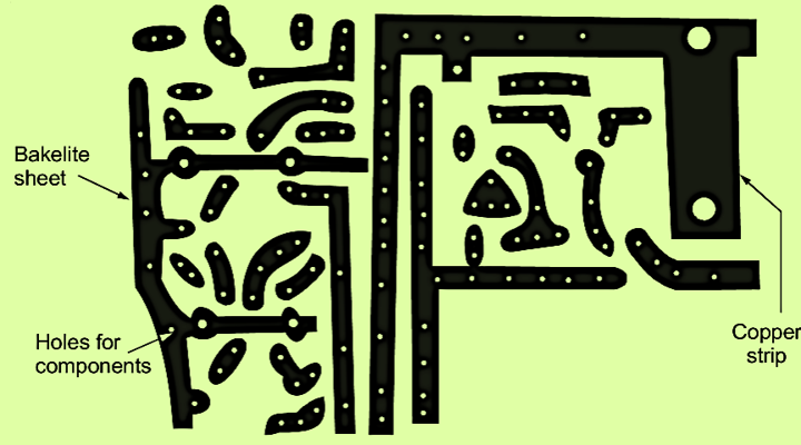
Fig. 1 A Printed Circuit Board
The exact manufacturing technique of PCB is described in the subsequent chapters.
Note: The PCB is also known as Printed Wiring Board. (PWB) or bprinted Board’ or simply Hence forth, the term “Board” will mean a PCB/PWB. Figure 1. shows a simple PCB.
Surface Treatment of Printed Circuit Board (PCB)
For protection against harsh environment, surface treatment of PCB is carried out as follows:
(1) A mask (covering layer) of sonic green lacquer is provided on the whole path of the current flow (copper track) except the solder points. This is called green masking. This has the following advantages:
- It is non-hygroscopic and protects against moisture and dampness.
- It is fire retardant
- It has high working temperature
- It has high insulating resistance
- By virtue of its use, stray capacitance is reduced
- Voltage handling capacity of the copper track is improved
(2) A superior insulating material (like epoxy) may be used for making a PCB. It also helps in protection of PCB against harsh environment.
(3) Copper for making tracks should be tinned (the process of mixing tin in proper percentage in copper is known as tinning). This prevents formation of copper oxide and provides protection against harsh environment.
(4) The copper track is dipped into solution of ferric chloride (Fe2Cl3) with few drops of hydrochloric acid (HCI). It also helps ¡n protecting the PCB against harsh environment.
(5) It is desirable to provide protection for PCB against dish, dust, contamination, humidity and mechanical troubles. The important insulating creatings are epoxy, polyurethanes, silicones, acrylics. Polystyrenes and varnishes. In selecting a coating material, its following characteristics should be considered:
- Efficiency to protect printed wiring insulation
- The effect of humidity and temperature on insulation resistance
- Electrical properties like dielectric constant, Q-Factor, etc.
- Flexibility
- Resistance against cracking
- Ease of application
- Transparency
- The ease by which it can be removed for repair of the boards.
Advantages of Printed Circuit Board (PCB)
Today PCB is the heart of every electronic instrument in entertainment as well as sophisticated fields. The reasons for popularity of PCBs are:
- PCB provides support for circuit components and interconnects the components electrically.
- It avoids bulk wiring and reduces weight of interconnection wiring.
- It is neat way of routing conductors.
- Location of parts is fixed allowing easy identification and as a result colour coding is climinated.
- Assembly errors are minimized due to accurate component mounting.
- It provides high design tiexibility.
- Complexity, time and cost of testing. checking process and maintenance of electronic equipment are reduced and simplified.
- The copper strips over the PCB serve the purpose of wires, hence use of lengthy wires is saved.
- Copper strips tightly fixed over the PCB and components are soldered with these strips. It gives tight connections which otherwise is not possible.
- Much time is saved in assembling the circuit over PCB as compared to the conventional method.
- As components are tightly fixed, risk of sort circuiting is minimzed.
- Use of PCB saves space unlike in a conventional assembly.
Disadvantages of Printed Circuit Board (PCB)
- Good amount of skill is required for designing and fabrication of PCBs
- As copper strips are very thin, PCBs cannot be used in circuits requiring heavy currents because in the case the strips will be heated and can cause problems.
- Soldering needs precaution as there is a risk of strips being overheated and destroyed.
- PCB cannot be used for very large circuits as it cannot carry heavy components. and also the cost and size of PCB in that case will be unbearable. Now the integrated circuits (I.C.s) are fast replacing the PCBs.
Precautions While Soldering A Printed Circuit Board (PCB)
As discussed above the copper strips of PCB are very thin. During soldering they may burn away due to overheating. Therefore while soldering a PCB, following precautions should be kept in mind:
- Erase out the layer of insulation if any, from the PCB.
- For the wiring, use a soldering ¡ron of lower wattage. For PCB soldering do not use an iron of more than 35 W.
- Do not keep soldering iron on a strip for more than the time required.
- Use small solder so that risk of short circuiting ofjoints with each other is minimum.
- If a strip breaks out, do not fill it with solder but join its two ends with a tinned wire.