In this topic, you study how to design Binary to BCD Code Converter Circuit and draw the logic diagram.
Truth table
The input is a 4-bit binary code (A B C D) so 16 (${2^4}$) combinations are possible. Hence the output should have 8-bit, but first three bits will all be a 0 for all combinations of inputs, the output can be treated as 5-bit BCD code (W X Y Z E). The conversion of binary code into BCD code as shown in
truth table 1,
Table 1: Binary to BCD Code Code Converter.
| Binary Code (Input) | BCD Code (Output) | |||||||
| A | B | C | D | W | X | Y | Z | E |
| 0 | 0 | 0 | 0 | 0 | 0 | 0 | 0 | 0 |
| 0 | 0 | 0 | 1 | 0 | 0 | 0 | 0 | 1 |
| 0 | 0 | 1 | 0 | 0 | 0 | 0 | 1 | 0 |
| 0 | 0 | 1 | 1 | 0 | 0 | 0 | 1 | 1 |
| 0 | 1 | 0 | 0 | 0 | 0 | 1 | 0 | 0 |
| 0 | 1 | 0 | 1 | 0 | 0 | 1 | 0 | 1 |
| 0 | 1 | 1 | 0 | 0 | 0 | 1 | 1 | 0 |
| 0 | 1 | 1 | 1 | 0 | 0 | 1 | 1 | 1 |
| 1 | 0 | 0 | 0 | 0 | 1 | 0 | 0 | 0 |
| 1 | 0 | 0 | 1 | 0 | 1 | 0 | 0 | 1 |
| 1 | 0 | 1 | 0 | 1 | 0 | 0 | 0 | 0 |
| 1 | 0 | 1 | 1 | 1 | 0 | 0 | 0 | 1 |
| 1 | 1 | 0 | 0 | 1 | 0 | 0 | 1 | 0 |
| 1 | 1 | 0 | 1 | 1 | 0 | 0 | 1 | 1 |
| 1 | 1 | 1 | 0 | 1 | 0 | 1 | 0 | 0 |
| 1 | 1 | 1 | 1 | 1 | 0 | 1 | 0 | 1 |
Drawing of K-map for each output
From this truth table, the K-maps are drawing shown in Figure 1, to obtain a minimized expression for each output.
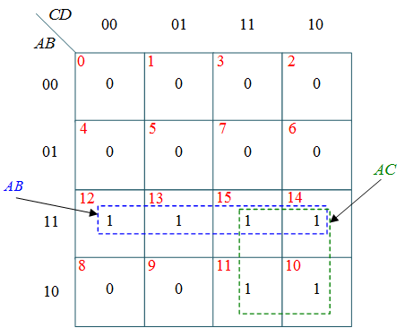
(a) k-map for W
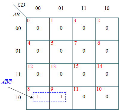
(b) k-map for X
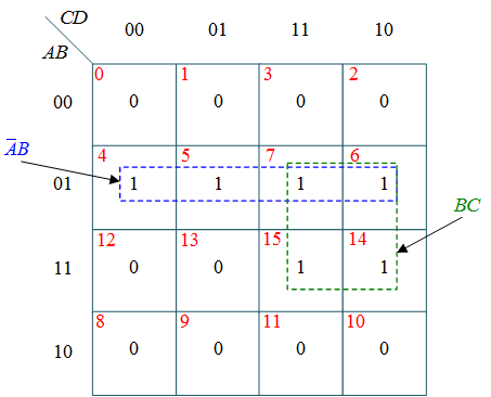
(c) k-map for Y
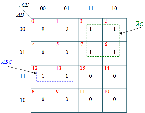
(d) k-map for Z
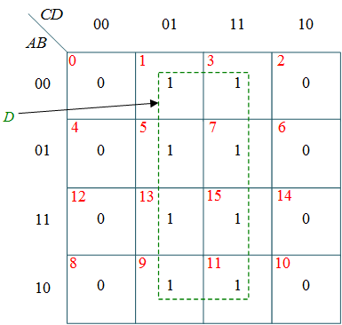
(e) k-map for E
Figure 1: k-maps for Binary to BCD Code Converter.
Minimized Expression for each output
The minimized expression for each output obtained from the K-map are given below as
$W = AB + AC$
$X = A \bar B \bar C $
$Y = \bar A B + B C $
$Z = AB \bar C + \bar A C $
$E = D $
Logic Circuit Diagram
Based on the above given minimized expression for each output, a logic circuit can be drawn as shown in Figure 2.
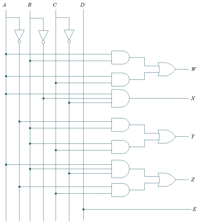
Figure 2: Binary to BCD Code Converter logic diagram.