In this topic, you study Depletion Region in PN junction diode – Definition, Theory & Diagram.
The movement of charge carriers across the junction creates a layer of immobile ions on each side. This layer is called depletion layer. The depletion region is shown in Fig. 7.4 (a).
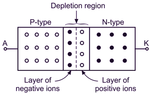
(a) Equal doping densities
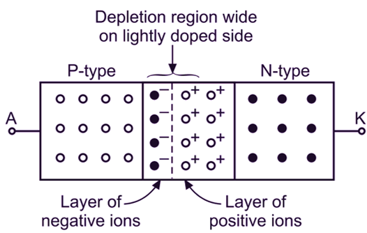
(b) Unequal doping densities
Fig. 1: Depletion region
On the N-side, the depletion region consists Of donor impurity atoms which give free electrons associated with them (lost negative charge) and becomes positively charged. The depletion region on the P-side is made up of acceptor impurity atoms which became negatively charged by loosing the hole associated with them (hole is filled by electron). When both the semiconductor materials have an equal doping concentration, the depletion layers on each side have equal widths. See Fig. 1(a). If P-type is heavily doped than N-type the width of the depletion layer is more into N-type in order to include an equal number of impurity atoms on each side of the junction. See Fig. 1 (b). And when the N-side is heavily doped than P-type, then depletion layer width is more in P-region than N-region. It means that the depletion region penetrates more in lightly doped region.