The Shunt Capacitor Filter comprises of a large value capacitor, which is connected in parallel with the load resistor.
Working of Shunt Capacitor Filter
Fig. 1 (a) shows the simplest and cheapest Shunt Capacitor filter arrangement to reduce the variations from the output voltage of a rectifier. The working of the shunt capacitor filter can be understood with reference to waveforms shown in Fig. 1 (b) to (d). Figure 1 (b) gives the wave shape of the AC input voltage. Output wave shapes without a filter capacitor and when it is connected across the output are shown in Fig. 1 (c) and (d) respectively.
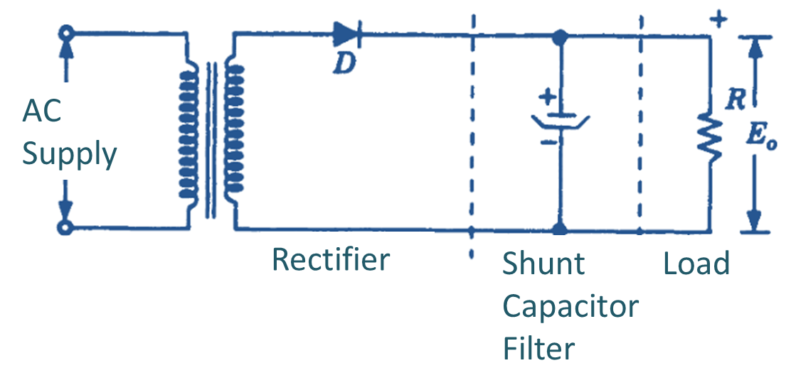
(a) Circuit Diagram
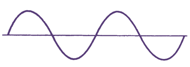
(a) Input voltage (AC Supply) waveform.
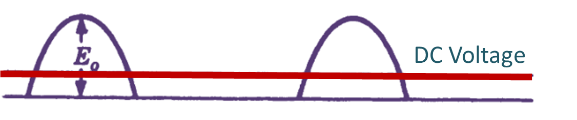
(b) Rectified output voltage without capacitor filter.
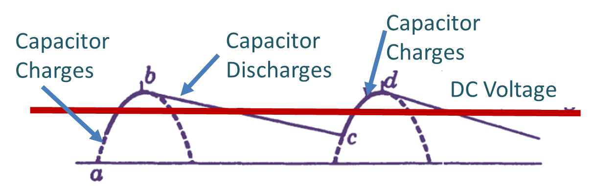
(c) Rectifier output with shunt capacitor filter.
Fig. 1: Half Rectifier with Shunt Capacitor Filter
A reference to Fig. 1 (d) shows that during positive half cycle of the input voltage, the rectifier conducts and supplies current to the load. The capacitor starts charging during this period and charges to the peak value of the input voltage. The charging period of the capacitor is marked (a, b) in Fig. 1 (d). As the input voltage crosses its peak point, the voltage at the rectifier plate becomes less than the cathode potential which is still maintained at a high positive potential because of the capacitor voltage. As a result, the diode gets reverse biased and the load is disconnected from the supply line due to diode which acts as open switch. Under this condition, the capacitor starts discharging through the load resistor and thus a voltage is maintained across the load resistor even during non-conducting period of the rectifier. Non conducting period of the rectifier which is also the discharge period of the capacitor is shown in Fig. 1 (d) as (b, c). The capacitor therefore helps in maintaining a voltage across the load at all times. The average value (DC) of the load voltage is increased with a corresponding decrease in the alternating ripple components.
The value of the filter capacitor is so choosen as to provide a low resistance path to the alternating components. For DC, the capacitor acts as an open circuit. Because of low reactance path provided by the capacitor, the alternating components are by-passed to ground.
Value of Shunt Capacitor Filter
The value of time constant CR has a pronounced effect on the performance of the filter. If capacitor is large. it will store more energy during conduction period. It can then supply larger current to the load during non-conduction period, thereby tending to maintain load voltage steadier. The average DC voltage is also increased.
If load resistor R is made large, the load current becomes less. Thus the current drawn from the capacitor during non-conduction period is also reduced. As a result, the output voltage becomes steadier and more. When the capacitor is reasonably large, the output voltage decays only slightly and ripple component is very low. Approximate value of ripple factor is then given
Ripple factor with shunt capacitor filter
\[RF=\frac{\pi }{\sqrt{3}}\times \frac{{{X}_{C}}}{R}=\frac{1}{2\sqrt{3}fCR}\]
where f is the ripple frequency. For half wave rectifiers, f is same as supply frequency but for full wave rectifier circuits, the ripple frequency is twice the supply frequency.
From the above discussion, a point that emerges is that we can obtain a much more steadier load voltage, if a capacitor with a very large value is used. But a very large value capacitor will require a large charging current and the rectifier diode must be capable of supplying this current. The maximum value of current that a diode can safely give is specified by diode manufacturers. This sets a limit on the maximum value of the capacitance that can be used as a shunt capacitor filter.