Design for manufacturing ¡s a new technique of designing. Manufacturability of PCBs depends upon its design. In a normal manufacturing process data flows only in one direction, i.e., ‘from design to manufacturing’ but DFM ensures that the date flows ‘from manufacturing to design’ also. This gives improved manufacturability of a board.
The DFM is a new design technique. Actually, it consists of a set of techniques to design a product in such a way that the cost and time to manufacture the product reduces to minimum. For this, interaction between designer and manufacturer at all the stages (starting from the beginning) is essential.
Proper feedback from the manufacturer to the designer about the problems faced by him during manufacturing is also important for a ‘cost effective’ designing.
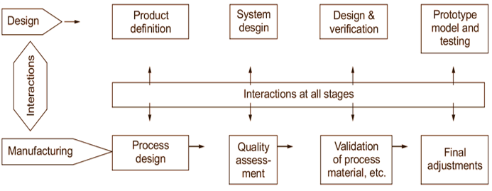
Block Diagram of Design for Manufacturing (DFM)
Figure 1 shows the block diagram of the DFM technique.
Advantages of Design for Manufacturing (DFM) Technique
The DFM technology has following advantages:
- Improved quality and better reliability of the product
- Reduced time to fabricate the product
- Few errors
- Reduced production costs
- A long life with trouble free service
- Reduced maintenance costs.
Guidelines For Design for Manufacturing (DFM)
- The DFM technique is a new approach to PCB designing; and while adopting this technique, the following guidelines will be helpful.
- PCB layout should be done keeping in mind the size of the laminate sheet available in the concerned industry, so that maximum utilization of the laminate sheet may be possible.
- Any plated through hole under a surface mounted component should be ‘solder masked’ to avoid any short circuits.
- Size of pad should be made just equal to the required size, as a bigger size results in ‘bridging, and a smaller size results in the problem of dry solders. The pad size should also match with the leads of the components.
- Hole diameter for thru’ hole components should also be just sufficient to allow capillary action of the solder. A larger diameter of the hole will increase consumption of the solder and small diameter results in dry solder joints.
- The variety of components should be minimum, e.g.. an ASIC can replace several small I.Cs which naturally will minimize the cost. Moreover. uniform orientation of all the components on the board also simplifies assembly and testing of the product.
- Sufficient margin on all sides of the PCB and sufficient spacing between the components also simplify automatic insertion of the components and their soldering.
- Proper component spacing and their uniform orientation help in minimizing exposure to the ‘wave’ during wave soldering. Moreover, if nitrogen wave soldering is used, problem of excess solder ¡s eliminated.