Diode is the most fundamental two terminal non-linear circuit element. The relationship between the current flowing through the diode and the voltage appearing across it is nonlinear. In other words, the diode has non-linear V-I characteristics.
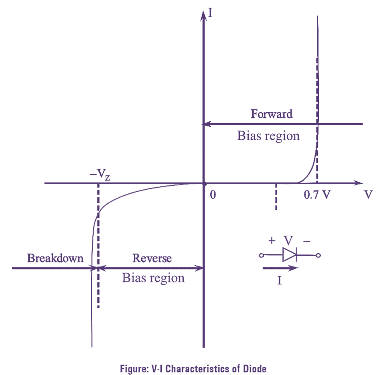
Figure illustrates the V-I charactefistics of a PN-junction diode. The charactefistics curve contains three distinct regions as,
- Forward bias region
- Reverse bias region
- Breakdown region.
Forward Bias Region: On forward biasing, P side of the PN-junction is connected to the positive of the voltage supply and N side of the PN-junction is connected to the negative of the voltage supply. Simply, forward bias region is the characteristics of the diode for V > 0. From figure it can be seen that (in the FB region) initially, the diode current is very small because the barrier potential prevents the flow of current through it. If the applied voltage exceeds the barrier potential, then for a small increase in the voltage produces a shall) increase in the current. The voltage at which the current starts to increase rapidly is called cut-in or knee voltage of the diode. It is denoted as Vγ.
For silicon diode Vγ = 0.7 V and Germanium diode Vγ = 0.3V.
Reverse Bias Region: On reverse biasing, P side of the PN-junction is connected to the negative terminal of the voltage supply and N side of the PN-junction is connected to the positive terminal of the voltage supply. Simply, reverse bias region is the characteristics of the diode for V < 0. From figure it can be seen that (in RB region) the diode current is very small, almost equal to zero for all values of voltage less than the break down voltage VZ. This is because in reverse bias the width of the potential barrier increases. As a consequence, the junction resistance becomes very high and practically no current flows through the circuit.
Breakdown Region: The diode enters the breakdown region when the magnitude of the reverse voltage exceeds a threshold value of that particular diode called the breakdown, voltage. In this region for very small variation in voltage the current increases rapidly as shown in figure. PN Diode should not be operated for VR > VBD because the diode will be damaged.
VI Characteristics of Ideal Diode
The deviation of V-I characteristics of pn junction diode from its ideal characteristics is illustrated below.
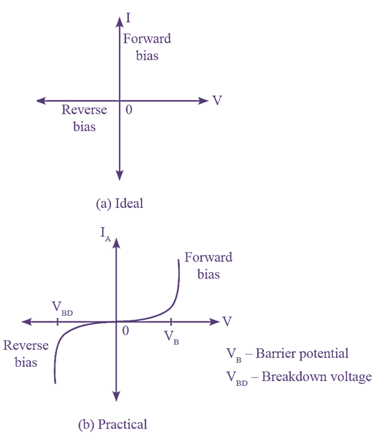
Figure 2.
The ideal and practical characteristics of p-n junction diode is shown in figure 2 (a) and (b) respectively.
1. When diode is forward biased.
(i) For ideal p-n diode, the forward resistance is zero. As a result, the diode acts as short circuit i.e., V = 0 and is remain unchanged for any value of ‘I’.
(ii) The practical p-n diode offers small forward resistance (i.e., static and dynamic resistance). Hence as voltage increases beyond barrier potential current also increases rapidly as shown in figure (b).
2. When diode is reverse biased.
(i) The ideal p-n diode offers infinite resistance. In this case the diode acts as open circuit i.e., current flowing through the diode is zero and the reverse voltage becomes infinite. An ideal diode does not undergo any breakdown, since the current is zero for any value of reverse voltage.
(ii) In a practical p-n diode, for an applied reverse voltage small amount of current flows due to minority charge carriers in both the regions. When the voltage increases above breakdown voltage (VBD). The maximum reverse saturation current flows in diode. As a consequence it gets destroyed.
Note: PN Junction diode should be operated for VR < VBD.