In this topic, you study Reverse Saturation Current of PN Junction Diode – Definition & Theory.
Practically no current flows due to majority carrier when the diode is reverse biased. However, a small amount of current does flow due to diffusion of minority carriers across the junction. The minority carriers are the hole-electron pairs generated in semiconductor material due to thermal energy. The current so produced is called reverse saturation current and is denoted by Io.
.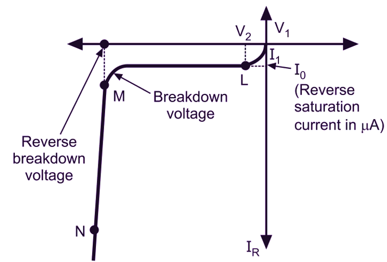
Fig. 1: Reverse Saturation Current of PN Junction Diode
The word saturation means that the reverse current cannot be increased by increasing the reverse bias across the diode (Figure 1). But it increases with increase in temperature. The reverse saturation current is of the order of nanoamperes (nA) for Silicon and microamperes (μA) for Germanium PN junction. The reverse saturation current, for Silicon devices, is smaller than that of Germanium because Silicon has a large energy gap (approximately 1.1 eV) between the conduction and valence bands. As a result of this, less number of minority carriers are thermally generated in Siliconthan Germanium at any temperature. The value of reverse of saturation current is about double in magnitude for every 10°C rise in temperature. For example, if for silicon Io is 5 nA at 25°C then it is approximately 10 nA at 35°C, 20 nA at 45°C, 40 nA at 55°C and so on. However, for germanium, Io is in the order of 1-2 μA at 25°C but its value increases to 100μA at 100°C.