A logic analyzer is a device that captures the data of the digital system and provide the display to the captured data for analysis.
Block Diagram of Logic Analyzer
The block diagram of a logic analyzer is shown in the figure below.
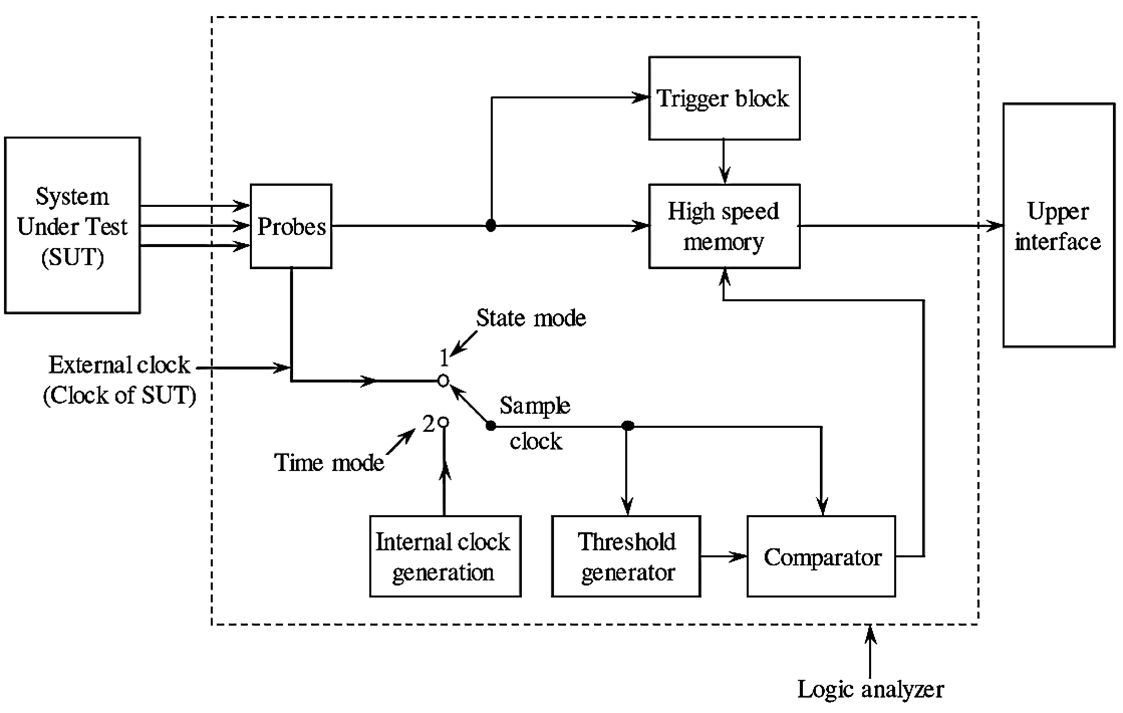
Figure 1: Block Diagram of Logic Analyzer
The main elements of a logic analyzer are probes, internal clock generator, threshold generator, comparator, memory, trigger block. Appropriate probes are used to connect the data lines of a digital system (i.e., System Under Test (SUT)) to the logic analyzer. The internal clock generator generates the clock pulses which are used for sampling the input data, The comparator block compares the sampled data and a specified threshold voltage generated by threshold generator. The memory of the logic analyzer is used to store the data captured by logic analyzer.
Working of Logic Analyzer
After receiving the signal from the system tinder test SUT, it samples the input signal at certain clock frequency. In the sampling process, it compares the input signal with a certain threshold voltage at each sample point (i.e., at each clock pulse) and depending upon the result of comparison it converts the input signal at that sampling instant into a logic 1 (High) or logic 0 (low) state. If the level of input signal is higher than the threshold voltage it is recognized as logic-I and if its level is less then the threshold level it is recognized or logic 0. Thus, by sampling process the input signal gets converted into a pattern of 0’s and l’s (i.e., the sampled data is a series of 0’s and 1 ‘s). The sampled data is then stored in the memory of logic analyzer with each sample point occupying a single memory location.
Types of Logic Analyzer
The logic Analyzer may be of two types:
- Logic Timing Analyzer (Asynchronous Measurements)
- Logic Analyzer (Synchronous Measurement)
Logic Timing Analyzer (Asynchronous Measurements)
This Analyzer “samples” the waveform at each edge of the internal clock generated at regular intervals of time stores them in memory and displays the same in a timing waveform. This is called as “asynchronous” measurement since the internal clock runs asynchronous to the logic system being tested.
Logic Analyzer (Synchronous Measurement)
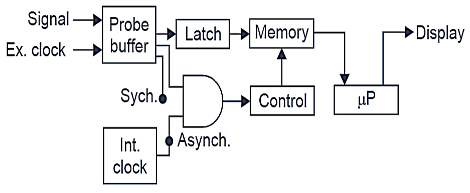
Fig. 1. Logic analyzer Synchronous Measurement.
This uses a signal from the circuit under test, external clock determines when the logic signal is to be stored. This is called as “synchronous” measurement since the external clock runs synchronous to the logic system being tested. Modern logic analyzer combines both the above functions in one unit.
The Fig. 1. shows block diagram of a logic analyzer. It combines both functions i.e., asychronous and synchronous. The logic signal data to be measured enters the Analyzer through “Probe Buffer”. The output from the buffer is clocked into a latch at regular intervals. The latched data is stored in the memory and is displayed by the microprocessor (µP).
The signal data used to latch can be obtained from two different sources. For asynchronous operation an internal clock is used and for synchronous operation, an external clock is used.
Applications of Logic Analyzer
A logic analyzer has the ability to capture and display the data of multiple digital signals (usually more than eight) at a time. Hence, a logic analyzer can be used to examine a large number of digital signal lines of a digital system.
Note: The logic probe can view only one signal at a time and also it cannot store it. When it is required to have a record of more than one signal simultaneously e.g., when it is necessary to look at the logic levels of all the lines of a microprocessor bus, we use a “logic Analyzer”.