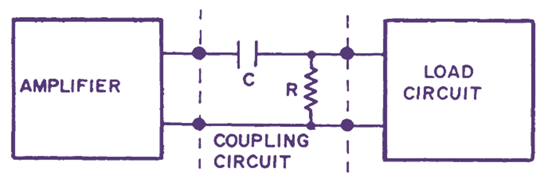
Fig. 1. RC coupling.
RC Coupling is the simplest and cheapest type of coupling scheme as shown in Fig. 1 and consists of a series coupling capacitor between the amplifier output points and the load circuit. The load may be a simple resistor, a loudspeaker, an antenna in case of a transmitter or another amplifying stage but RC coupling is generally used when a second amplifying stage is used as a load. The series capacitor acts as a short circuit for signal frequencies thereby passing the entire signal to the output, but for DC the capacitor behaves as open circuit. Therefore DC is not passed to the output.
Two Stage Transistor RC Coupled Amplifier
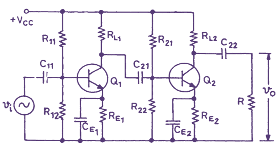
Fig. 2. Schematic diagram of a two-stage RC coupled amplifier.
An outline of this coupling scheme has been given in Fig. 1. In this scheme, a resistor is used as the collector load of an amplifier stage and signal output from this stage is given to the base of the second stage which acts as load to the first stage. Fig. 2 shows the schematic arrangement of a two stage transistor RC coupled amplifier.
As can be seen from circuit (R11, R21, RE1) and (R12, R22, RE2) provide self bias to the two stages. RL1 and RL2 are the collector loads and C11, C21 and C22 are the coupling capacitors. C11 Couples the input signal to the base of Q1. C21 Couples the signal output to the base of Q2 while C22 connects the output to the load resistor R.
The input impedance of the second stage of the amplifier acts as load for the first stage. Thus, if we calculate the gain of the first stage separately, it will have a higher gain but when second stage is connected, then AC load of the first stage becomes collector load RL1 shunted by the input impedance of the second stage. Because of the shunting effect of this impedance, the voltage gain of the first stage is reduced. Thus, while calculating gain of different stages of a multi-stage amplifier, shunting effect of the input impedance of the following stage must be taken into account, if the results are to be accurate.
Frequency Response of RC Coupled Amplifiers
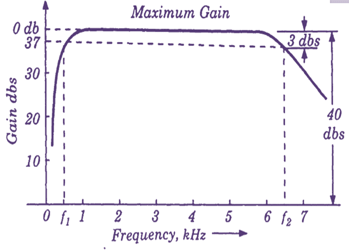
Fig. 3. Frequency response of a RC coupled amplifier.
RC coupled amplifiers are most commonly employed for amplification of audio frequencies. Since these signals contain a band of frequencies starting from a low frequency of a few Hz to a high frequency of several kHz, it is desired that all these signal components should be amplified equally. However, in actual practice, this does not happen and the amplification is found to become less at very low and at high frequencies. A plot of voltage gain of the amplifier versus signal frequency gives a true picture of the amplifier performance and is termed as the frequency response of the amplifier. The response curve of an RC coupled amplifier is shown in Fig. 3. It can be seen from the response curve that the voltage gain is maximum and constant in the mid frequency region. At very low and very high signal frequencies, the voltage gains fall off to a low value.
Fall of Voltage Gain at Low Frequencies
While calculating voltage gain of an amplifier in the previous sections, it was assumed that coupling capacitors C1 and C2 as well as emitter capacitor CE offer negligible reactance and may be considered as short circuit. However, this assumption is not valid for all signal frequencies since the reactance of a capacitor is given as,
\[{{X}_{C}}=\frac{1}{2\pi fC}\]
Thus, when signal frequency becomes low, the reactance of all these capacitors increases and can no longer be neglected.
Fall of Voltage Gain at High Frequencies
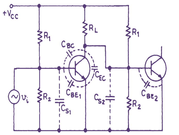
Fig. 4. Effect of device capacitances and stray capacitances at high frequencies of the signal.
The voltage gain of an amplifier is found to reduce at high signal frequencies also. There are two factors responsible for this. Firstly, it is found that the current amplification factor β of a transistor begins to fall if signal frequency is increased sufficiently. Another important factor responsible for the reduction of voltage gain at high frequencies is the presence of device capacitances and stray shunt capacitances. These capacitances are shown in Fig. 4.