The transistor when used as a switch must, therefore, be able to operate in cutoff region (open switch) and saturation region (closed switch) only.
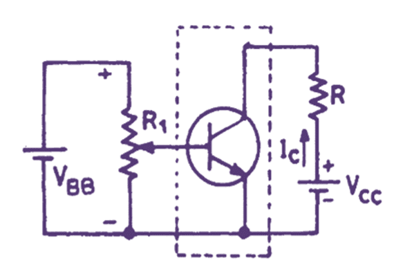
(a) A CE transistor used as a rehostat to control current in the load.
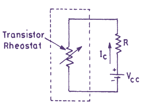
(b) Equivalent circuit.
Figure 1: Transistor as a Switch.
Consider the circuit given in Fig. 1 (α). The circuit consists of a load resistor RL fed from a battery VCC the transistor is connected in the path of the current flow.
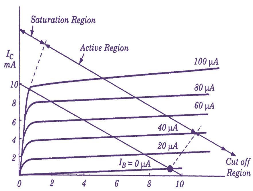
Fig. 2. DC load line drawn to show the linear variation of load current.
The load line for this circuit is drawn in Fig. 2 and it can be seen that current through the load can be varied from zero to a maximum value dependent upon the load value and this variation in the current is obtained by varying the base current of the controlling transistor. Thus when IB = 0, collector current flowing through the load is zero (if the leakage current ICBO is neglected). This corresponds to a rheostat set to maximum resistance (infinity) and lies at the intersection of the load line with the characteristic curve for IB = 0.
If the base current is increased, the load current will correspondingly increase. This increase is along the load line. Similarly, when the base current is made large, the transistor becomes saturated; the collector current will become maximum and may have a value limited by load resistance only. This corresponds to rheostat set to zero resistance in the equitant circuit shown in Fig. 1 (b) and lies at the intersection of the load line with characteristic curve for IB = 100 µA. For all other values of the base current,
The load current will vary along the load line. The load current can be controlled to any value by properly adjusting the base current of the transistor and the transistor may be considered as a rheostat having resistance variation from zero to infinity.
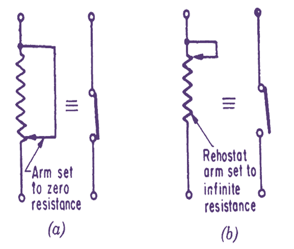
Fig. 3. Transistor rheostat used as (a) closed switch (b) open switch.
A transistor can be made to work as a rheostat with a resistance that may be set to any value between zero and infinity. If the transistor is set to offer zero resistance it may be considered as a closed switch. Similarly, if the transistor rheostat is set to offer infinite resistance, the current stops to flow and the transistor may be considered to have acted as an open switch. Fig. 3 shows the positions of a transistor rheostat to act as a closed switch and as an open switch.
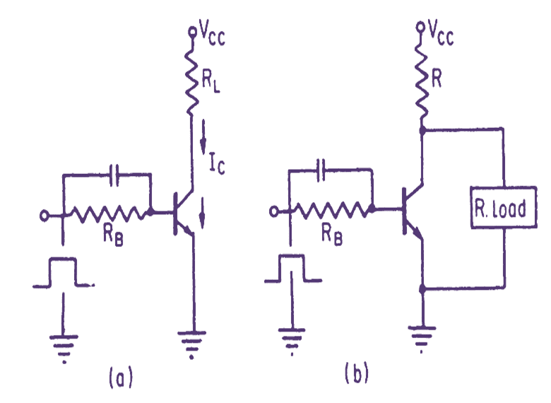
Fig. 4. Transistor switches used as (a) normally OFF switch (b) normally ON switch.
The transistor when used as a switch, the change over from cutoff region to saturation region and vice versa has to be fast if the transistor is to replace an ordinary switch and for this reason, current in the form of a rectangular pulse must be fed to the base. The transistor switch will remain closed as long as the input pulse is present and when the pulse ends, the current stops and transistor switch is open circuited. Fig. 4 shows the use of a transistor to act as (a) normally OFF and (b) normally ON switch.
A resistance RE is usually added in series with the base so as to limit the base current and avoid any damage to the emitter-base junction. But the addition of this resistance does not allow the base current to shoot up sharply and thus switching action is delayed. It is, therefore, a normal practice to connect a capacitor in shunt with this resistance as shown in Fig. 4. When the base current pulse rises from zero to maximum or falls from maximum to zero, the capacitor acts as short circuit for these changing currents. The resistance RB is thereby effect lively shorted by the capacitor and rise or fall in the base current is therefore instant and delay is eliminated. This capacitor is, therefore, referred to as Speed up Capacitor.
Load to a transistor switch may be connected in two ways as shown in Fig. 4.
When the load is in series with the transistor, the current through the load is same as the collector current of the transistor as shown in Fig. 4 (a). When the load is placed in shunt with the transistor, the action is reversed. When there is no input pulse at the transistor base, current flows through the load. With the application of a base current pulse, the transistor switch becomes ON and load is effectively short circuited and whole of the current is by passed through the transistor.
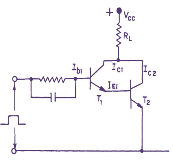
Fig. 5. A solid state switch capable of switching heavy load current.
If the external load requires a higher current which cannot be supplied by a single transistor, two transistors may be connected in cascade to increase the current carrying capacity of the transistor switch. The arrangement commonly used for switching ON/OFF heavier load currents by means of a transistor switch is given in Fig. 5.
In this arrangement, two transistors are employed such that the emitter current of the transistor T1 is used as the base current for T2. T2 Transistor is a device selected to have high current rating. If β1 and β2 are assumed to the current amplification factors of transistor T1 and T2 respectively, then the base current Ib1 is amplified by times before being fed to base of T2. In T2, it is amplified by times. Thus load current IL given as,
\[{{I}_{L}}={{I}_{C}}_{1}+{{I}_{C}}_{2}\]
\[{{I}_{L}}={{\beta }_{1}}.{{I}_{{{B}_{1}}}}+{{\beta }_{2}}.{{I}_{{{B}_{2}}}}\]
\[{{I}_{L}}={{\beta }_{1}}+{{I}_{{{B}_{1}}}}+{{\beta }_{1}}.{{\beta }_{2}}.{{I}_{{{B}_{1}}}}\]
Also
\[{{I}_{L}}\simeq {{\beta }_{1}}.{{\beta }_{2}}.{{I}_{{{B}_{1}}}}\]
Thus, with a small value of base current IB1 we are able to switch large value of load current. This arrangement is often referred to as Darlington connection.