The SCR is a PNPN semiconductor switching device. It can be considered to be constructed by sandwitching two complementary transistors one PNP and the other NPN type. Fig. 1 (a) shows the structure of two transistor model of SCR.
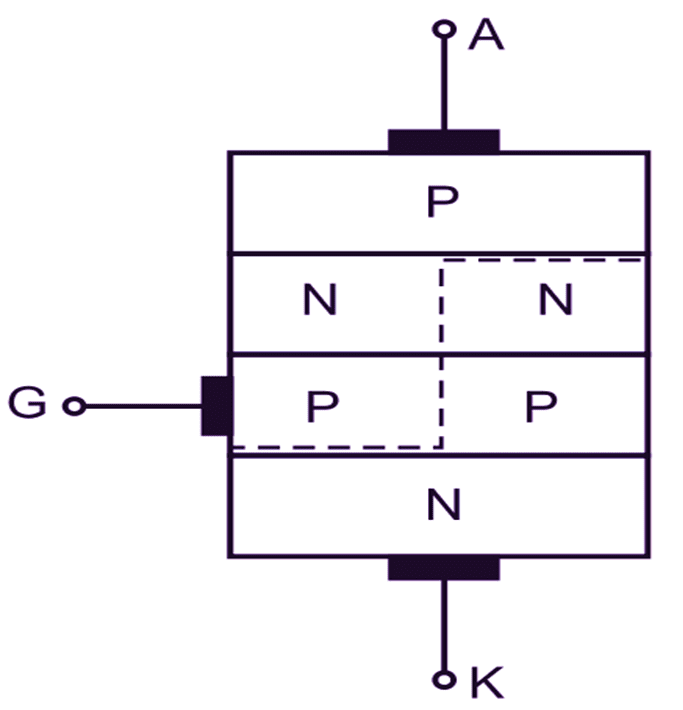
(a) Structure.
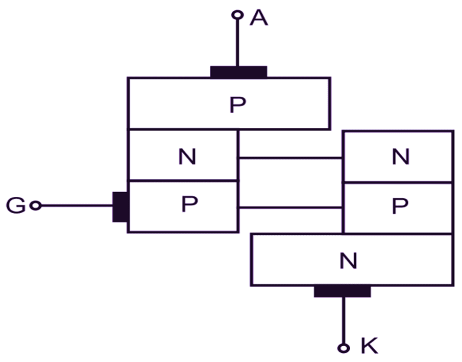
(b) Equivalent structure.
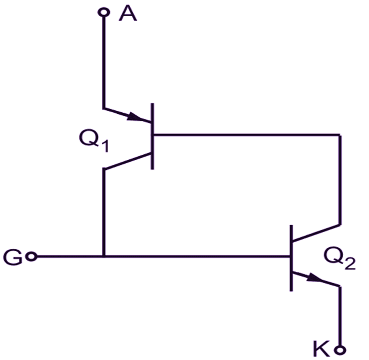
(c) Equivalent circuit
Fig. 1: Two transistor model of an SCR.
Two transistor model of an SCR is obtained by splitting two middle layers into two separate parts as shown in Fig. 1 (b). The corresponding symbolic representation of two transistor model of an SCR is shown in Fig. 1 (c). It may be noted that the anode is connected to the emitter of a PNP transistor and the cathode is connected to the emitter of an NPN transistor. The collector of each transistor is connected to the base of other transistor. Both the transistors are connected in common base configuration. A current loop is formed in the inner layers of the SCR and this loop is responsible for regenerative feedback action.
Two Transistor Model of SCR Operating principle
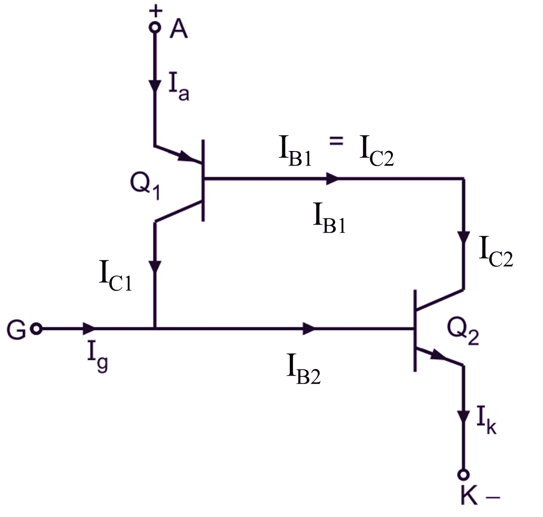
Fig. 2: Equivalent circuit for two transistor model of an SCR.
The operating principle of an SCR, i.e. how the SCR turns ON by the internal regenerative feedback, can be best understood by two transistor model of an SCR.
The electrical equivalent circuit for two transistor model of an SCR is shown in Fig. 2. The SCR is forward biased by applying a supply voltage VS. Assume that the supply voltage is less than the breakover voltage VBO, i.e. VS < VBO and the SCR is not triggered. As both the transistors Q1 and Q2 are connected in CB configuration, the collector current IC is given by
\[{{\text{I}}_{\text{C}}}=\text{ }\!\!\alpha\!\!\text{ }{{\text{I}}_{\text{E}}}+\text{ }{{\text{I}}_{\text{CBO}}}\]
A small gate current will increase the loop currents, i.e. base currents and collector currents (IB1, IB2, IC and IC2) of both transistors cumulatively so that the anode through the SCR will increase sharply. This can be explained as below:
By Kirchhoffs current law (KCL), the anode current can be written as
\[{{\text{I}}_{\text{a}}}=\text{ }{{\text{I}}_{\text{C1}}}+\text{ }{{\text{I}}_{\text{C2}}}\]
Using CB configuration for both transistors, we get
\[{{\text{I}}_{\text{C1}}}=\text{ }{{\text{ }\!\!\alpha\!\!\text{ }}_{\text{1}}}{{\text{I}}_{\text{E1}}}+\text{ }{{\text{I}}_{\text{CBO1}}}\]
\[{{\text{I}}_{\text{C2}}}=\text{ }{{\text{ }\!\!\alpha\!\!\text{ }}_{\text{2}}}{{\text{I}}_{\text{E2}}}+\text{ }{{\text{I}}_{\text{CBO2}}}\]
where α1 and α2 are the current gains for transistors Q1 and Q2. ICBO1 and ICBO2 are the reverse saturation currents for transistors Q1 and Q2.
The anode current can be written as
\[{{\text{I}}_{\text{a}}}=\text{ }\left( {{\text{ }\!\!\alpha\!\!\text{ }}_{\text{1}}}{{\text{I}}_{\text{E1}}}+\text{ }{{\text{I}}_{\text{CBO1}}} \right)\text{ }+\text{ }\left( {{\text{ }\!\!\alpha\!\!\text{ }}_{\text{2}}}{{\text{I}}_{\text{E2}}}+\text{ }{{\text{I}}_{\text{CBO2}}} \right)\]
We know that IE1 = Ia and IE2 = Ik.
\[{{\text{I}}_{\text{a}}}=\text{ }\left( {{\text{ }\!\!\alpha\!\!\text{ }}_{\text{1}}}{{\text{I}}_{\text{a}}}+\text{ }{{\text{I}}_{\text{CBO1}}} \right)\text{ }+\text{ }\left( {{\text{ }\!\!\alpha\!\!\text{ }}_{\text{2}}}{{\text{I}}_{\text{k}}}+\text{ }{{\text{I}}_{\text{CBO2}}} \right)… (1)\]
By applying KCL, cathode current can be written as
\[{{\text{I}}_{\text{k}}}=\text{ }{{\text{I}}_{\text{B2}}}+\text{ }{{\text{I}}_{\text{C2}}}\]
As
\[{{\text{I}}_{\text{B2}}}=\text{ }{{\text{I}}_{\text{g}}}+\text{ }{{\text{I}}_{\text{C1}}}\]
\[{{\text{I}}_{\text{k}}}=\text{ }\left( {{\text{I}}_{\text{g}}}+\text{ }{{\text{I}}_{\text{C1}}} \right)\text{ }\!\!~\!\!\text{ }+\text{ }{{\text{I}}_{\text{C2}}}\]
Also
\[{{\text{I}}_{\text{a}}}=\text{ }{{\text{I}}_{\text{C1}}}\text{ }\!\!~\!\!\text{ }+\text{ }{{\text{I}}_{\text{C2}}}\]
\[{{\text{I}}_{\text{k}}}=\text{ }{{\text{I}}_{\text{g}}}+\text{ }{{\text{I}}_{\text{a}}}… (2)\]
Substituting equation (2) in equation (1), we get
\[{{\text{I}}_{\text{a}}}=\text{ }\left( {{\text{ }\!\!\alpha\!\!\text{ }}_{\text{1}}}{{\text{I}}_{\text{a}}}+\text{ }{{\text{I}}_{\text{CBO1}}} \right)\text{ }+\text{ }\left[ {{\text{ }\!\!\alpha\!\!\text{ }}_{\text{2}}}\left( {{\text{I}}_{\text{g}}}+\text{ }{{\text{I}}_{\text{a}}} \right)\text{ }+\text{ }{{\text{I}}_{\text{CBO2}}} \right]\]
\[{{\text{I}}_{\text{a}}}=\text{ }\left[ {{\text{ }\!\!\alpha\!\!\text{ }}_{\text{1}}}{{\text{I}}_{\text{a}}}+\text{ }{{\text{ }\!\!\alpha\!\!\text{ }}_{\text{2}}}{{\text{I}}_{\text{a}}} \right]\text{ }+\text{ }\left[ {{\text{ }\!\!\alpha\!\!\text{ }}_{\text{2}}}{{\text{I}}_{\text{g}}}+\text{ }{{\text{I}}_{\text{CBO1}}}+\text{ }{{\text{I}}_{\text{CBO2}}} \right]\]
Also
\[{{\text{I}}_{\text{a}}}-\text{ }{{\text{I}}_{\text{a}}}\left( {{\text{ }\!\!\alpha\!\!\text{ }}_{\text{1}}}+\text{ }{{\text{ }\!\!\alpha\!\!\text{ }}_{\text{2}}} \right)\text{ }=\text{ }{{\text{ }\!\!\alpha\!\!\text{ }}_{\text{2}}}{{\text{I}}_{\text{g}}}+\text{ }{{\text{I}}_{\text{CBO1}}}+\text{ }{{\text{I}}_{\text{CBO2}}}\]
where ICBO = ICBO1 + ICBO2 is the total reverse leakage current in collector-base junction.
Thus
\[{{\text{I}}_{\text{a}}}-\text{ }{{\text{I}}_{\text{a}}}\left( {{\text{ }\!\!\alpha\!\!\text{ }}_{\text{1}}}+\text{ }{{\text{ }\!\!\alpha\!\!\text{ }}_{\text{2}}} \right)\text{ }=\text{ }{{\text{ }\!\!\alpha\!\!\text{ }}_{\text{2}}}{{\text{I}}_{\text{g}}}+\text{ }{{\text{I}}_{\text{CBO}}}\]
Thus
\[{{\text{I}}_{\text{a}}}=\text{ }\frac{{{\text{ }\!\!\alpha\!\!\text{ }}_{\text{2}}}{{\text{I}}_{\text{g}}}+\text{ }{{\text{I}}_{\text{CBO}}}}{1-\left( {{\text{ }\!\!\alpha\!\!\text{ }}_{\text{1}}}+\text{ }{{\text{ }\!\!\alpha\!\!\text{ }}_{\text{2}}} \right)}\]
where (α1 + α2) is the loop gain.
In silicon transistors, the current gain α depends upon the emitter current and its value is approximately or less than 0.5. The SCR is made up of silicon, the current gain α is about 0.5 at low emitter current. When the SCR is not triggered, i.e. Ig = 0, the emitter current is negligibly small and hence α1 and α2 are very small, i.e. (α1 + α2) < 1.
So, the anode current can be written as
\[{{\text{I}}_{\text{a}}}=\text{ }\frac{{{\text{I}}_{\text{CBO}}}}{1-\left( {{\text{ }\!\!\alpha\!\!\text{ }}_{\text{1}}}+\text{ }{{\text{ }\!\!\alpha\!\!\text{ }}_{\text{2}}} \right)}…(3)\]
As (α1 + α2) is less than unity, the anode current will be negligibly small. The SCR does not conduct the current and remains OFF. This is a forward blocking state. When the forward biased SCR is triggered by applying a positive gate current pulse, the emitter currents in both transistors increase the current gains α1 and α2. When the loop gain (α1 + α2) increases and reaches the unity, the anode current increases rapidly to a high value as per equation (3). The SCR now conducts the current and turns it ON. This is a forward conduction (ON) state. Thus the SCR can be turned ON by passing a positive gate current so that the loop gain (α1 + α2) approaches to unity.