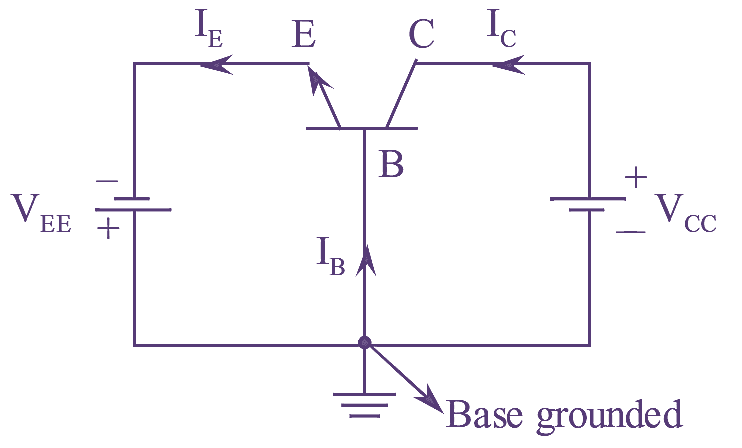
Figure 1: Common Base (CB) Configuration.
The configuration in which base is common to both the input and output sides is known as ‘common base configuration’.
An NPN transistor arranged in Common Base (CB) configuration is as shown in figure (l). In this connection the emitter, collector and base act as input, output and common terminals respectively. The base is at ground potential. Hence this configuration is also referred by the name grounded-base configuration. The voltages at the collector and emitter terminals are measured with respect to base.
Characteristics of Common Base (CB) Configuration
The arrangement of an NPN transistor in common base configuration is as shown in figure (2).
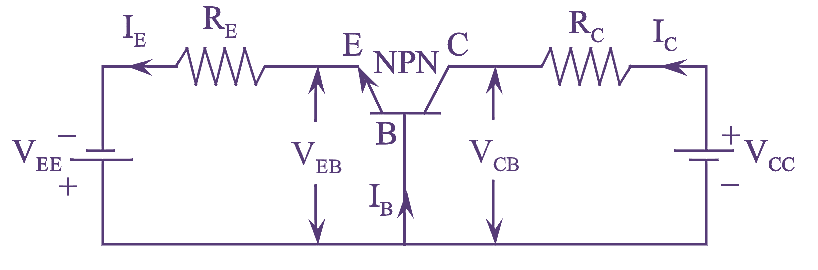
Figure 2: CB Configuration.
Input Characteristics
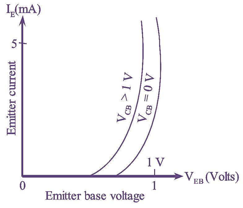
Figure 3: Input characteristics of CB transistor Configuration.
The curve plotted between emitter-base voltage (VEB) and emitter current (IE) keeping collector-base voltage (VCE) constant is known as input characteristics of CB transistor.
The input characteristics of BJT in common base configuration is as shown in figure (2). From figure (3), it can be observed that IE is the input current, VEB is the input voltage and VCB is the output voltage.
(i) Initially, the emitter-base junction of BJT is forward biased and VCB is kept at zero volts. The resultant input characteristics resembles with the forward characteristics of p-n diode, such that for a small increase in VBE a rapid increase in IE is observed.
(ii) On increasing the value of VCB from zero volts, keeping VEB constant, a decrease in the width of base region is observed. This effect is known as early effect. This intern increases the IE For every increase in VCB value, the curve shifts towards the left.
Output Characteristics
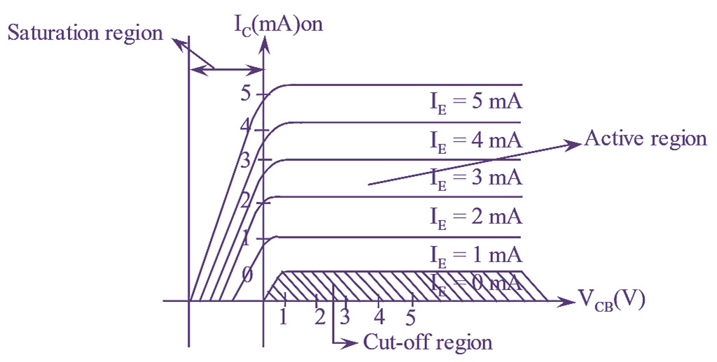
Figure 4: Output characteristics of CB transistor Configuration.
The curves plotted between collector- base voltage (VCB) and collector current (IC), keeping the emitter current (IE) constant is known as output characteristics of CB transistor.
The output characteristics of BJT in CB configuration is as shown, in figure (4). From figure (4), it can be observed that, IC is the output current, VCB is the output voltage and IE is the input current.
The output characteristics of a transistor are divided into three regions as shown in figure (4).
Active Region: In this region the emitter junction is forward biased and collector junction is reverse biased. It lies between the saturation and cut-off regions of transistor.
Saturation Region: In this region both the emitter and collector junctions are forward biased. It usually lies to the left of the ordinate VCB = 0.
Cut-off Region: In this region both the emitter and collector junctions are reverse biased. This region lies below IE = 0.
From the output characteristic curves it can be observed
(a) The collector current varies only for low values of VCB (i.e., < 1 V). At higher values of VCB, IC becomes constant as indicated by the straight parallel curves. Thus IC depends only on IE
(b) For large variation in VCB, only a small variation occurs in IC. This implies that there exists a very high value of output resistance.
Current Gain in Common Base (CB) Configuration
The ratio of collector current (IC) to the emitter current (IE) gives the common base D.C current gain of transistor. It is denoted by α, αdc or hfb and can be expressed as,
\[\alpha =\frac{{{I}_{C}}}{{{I}_{E}}}…(1)\]
Since IC is smaller than I therefore u is always less than unity.
Equation (1) can be rewritten as,
\[{{I}_{C}}=\alpha {{I}_{E}}…(2)\]
From the IE, IB and IC relationship,
\[{{I}_{E}}={{I}_{B}}+{{I}_{C}}…(3)\]
Since collector current IC is also produced by the thermally generated carriers as leakage current ICO. The total collector current is given as,
\[{{I}_{C}}=\alpha {{I}_{E}}+{{I}_{CO}}…(4)\]
\[\alpha {{I}_{E}}={{I}_{C}}-{{I}_{CO}}\]
\[\alpha =\frac{{{I}_{C}}-{{I}_{CO}}}{{{I}_{E}}}…(5)\]
Substituting equation (3) in eqautions (5),
\[\alpha =\frac{{{I}_{C}}-{{I}_{CO}}}{{{I}_{B}}+{{I}_{C}}}\]
\[\alpha ({{I}_{B}}+{{I}_{C}})={{I}_{C}}-{{I}_{CO}}\]
\[{{I}_{C}}=\alpha ({{I}_{B}}+{{I}_{C}}){{I}_{CO}}\]
\[(1-\alpha ){{I}_{C}}=\alpha {{I}_{B}}+{{I}_{CO}}\]
\[{{I}_{C}}=\frac{\alpha {{I}_{B}}}{1-\alpha }+\frac{{{I}_{CO}}}{1-\alpha }\]
This is the required output current i.e., collector current of a common-base transistor.