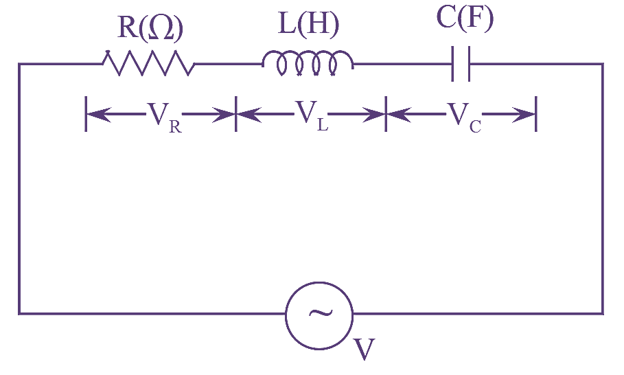
Figure (1): RLC Series Circuit.
An RLC series circuit consisting of a resistor ‘R’ Ohm (Ω) in series with an inductance of ‘L’ Henrys and capacitance of ‘ C’ Farads connected to an A.C supply as shown in figure (1).
Applying Kirchhoff’s voltage law to the above circuit,
\[V={{V}_{R}}+{{V}_{L}}+{{V}_{C}}=IR+I{{X}_{L}}+I{{X}_{C}}\]
Where,
V = Source voltage
VR = Voltage drop across resistor = IR
VL = Voltage drop across inductor = IXL
VC = Voltage drop across capacitor = IXC
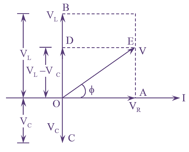
Figure (2): RLC Series Circuit Phasor Diagram when VL > VC.
The phasor diagram is drawn taking the current as the reference phasor as shown in figure (2).
From the phasors diagram
\[O{{E}^{2}}=O{{A}^{2}}+O{{D}^{2}}\]
\[{{V}^{2}}=V_{R}^{2}+{{\left( {{V}_{L}}-{{V}_{C}} \right)}^{2}}\]
\[V=\sqrt{V_{R}^{2}+{{\left( {{V}_{L}}-{{V}_{C}} \right)}^{2}}}\]
\[V=\sqrt{{{\left( IR \right)}^{2}}+{{\left( I{{X}_{L}}-I{{X}_{C}} \right)}^{2}}}\]
\[V=I\sqrt{{{R}^{2}}+{{\left( {{X}_{L}}-{{X}_{C}} \right)}^{2}}}\]
\[V=IZ\]
Where,
\[Z=\sqrt{{{R}^{2}}+{{X}^{2}}}\Omega \]
= Impedance of the circuit.
From the phasor diagram here, three cases arise.
- XL > XC i.e., XL – XC is positive
- XC > XL i.e., XL – XC is negative
- XL = XC i.e., XL – XC is zero.
Case (i): XL > XC
From the phasor diagram shown in figure (2), the net reactance is inductive. Therefore, for the condition XL > XC the circuit behaves like an inductive circuit. The current lags behind the voltage by 90º.
Net reactance,
\[X={{X}_{L}}-{{X}_{C}}\]
Impedance,
\[Z=\sqrt{{{R}^{2}}+{{X}^{2}}}\Omega \]
The phase difference between voltage and current,
\[\phi ={{\tan }^{-1}}\left( \frac{X}{R} \right)={{\tan }^{-1}}\left( \frac{{{X}_{L}}-{{X}_{C}}}{R} \right)\]
The power taken by the circuit,
\[P=VI\cos \phi \text{ watts}\]
Since pure inductance and capacitance do not consume power, power factor of the given circuit is $\cos \phi$ lagging.
Case (ii): XC > XL
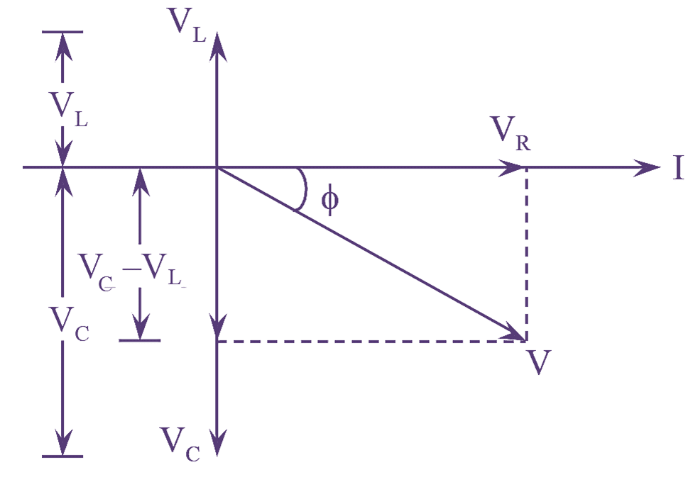
Figure (3): RLC Series Circuit Phasor Diagram when XC > XL.
From the phasor diagram shown in figure (3), the net reactance is capacitive. Therefore, for the condition XC > XL the circuit behaves like a capacitive circuit. The current leads voltage by 90º.
Net reactance,
\[X={{X}_{L}}-{{X}_{C}}\]
Impedance,
\[Z=\sqrt{{{R}^{2}}+{{X}^{2}}}\]
\[Z=\sqrt{{{R}^{2}}+{{\left( {{X}_{C}}-{{X}_{L}} \right)}^{2}}}\Omega \]
The phase difference between voltage and current,
\[\phi ={{\tan }^{-1}}\left[ \frac{X}{R} \right]\]
\[{{\tan }^{-1}}\left[ \frac{{{X}_{L}}-{{X}_{C}}}{R} \right]\]
The power taken by the circuit,
\[P=VI\cos \phi \text{ Watts}\]
Power factor of the given circuit is $\cos \phi$ leading.
Case (iii): XL= XC
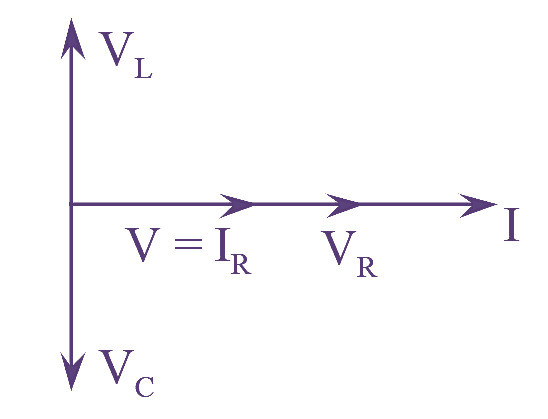
Figure (4): RLC Series Circuit Phasor Diagram when XL = XC.
From the phasor diagram shown in figure (4), the net reactance of the circuit for the given condition XL= XC is zero. The circuit behaves like a resistive circuit.
Net reactance,
\[X={{X}_{L}}-{{X}_{C}}\]
\[X=0\]
Impedance,
\[Z=\sqrt{{{R}^{2}}+{{X}^{2}}}\]
\[Z=\sqrt{{{R}^{2}}+0}=R\Omega \]
Power taken by the circuit,
\[P=VI\cos \phi \text{ Watts}\]
The phase difference between voltage and current is zero. Thus,
\[\phi = 0\]
Since the current is in phase with voltage, the power factor $\cos \phi$ is unity.