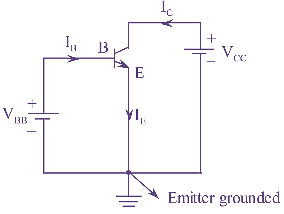
Figure 1: Common Emitter (CE) Configuration.
The configuration in which emitter is common to both sides of configuration is known as common emitter configuration.
An NPN transistor arranged in Common Emitter (CE) configuration is as shown in figure (1). In this connection the base collector and emitter act as input, output and common terminals respectively. The emitter is at ground potential. Hence this configuration is also referred by the name grounded-emitter configuration.
Characteristics of Common Emitter (CE) Configuration
The arrangement of an NPN transistor in common-emitter configuration is as shown in figure (2).
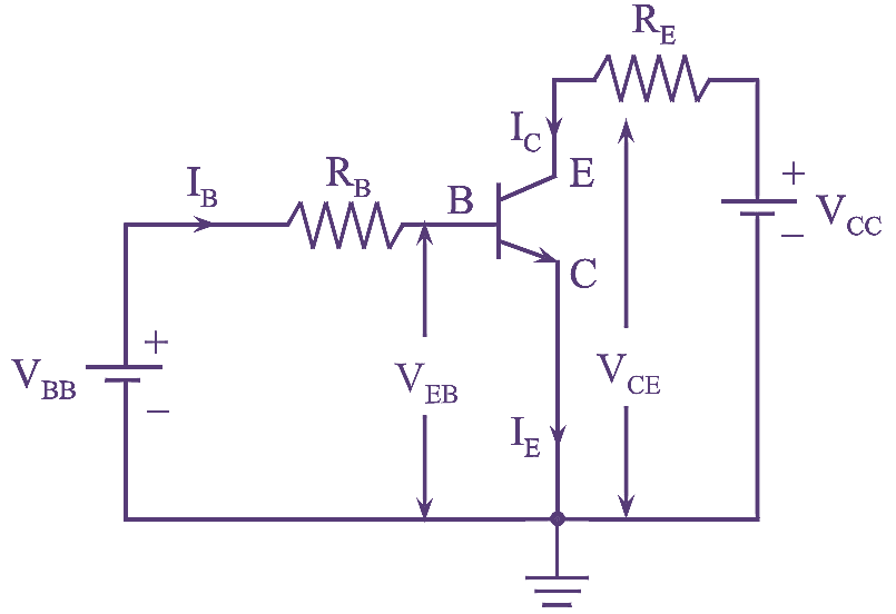
Figure 2: CE Configuration.
Input Characteristics
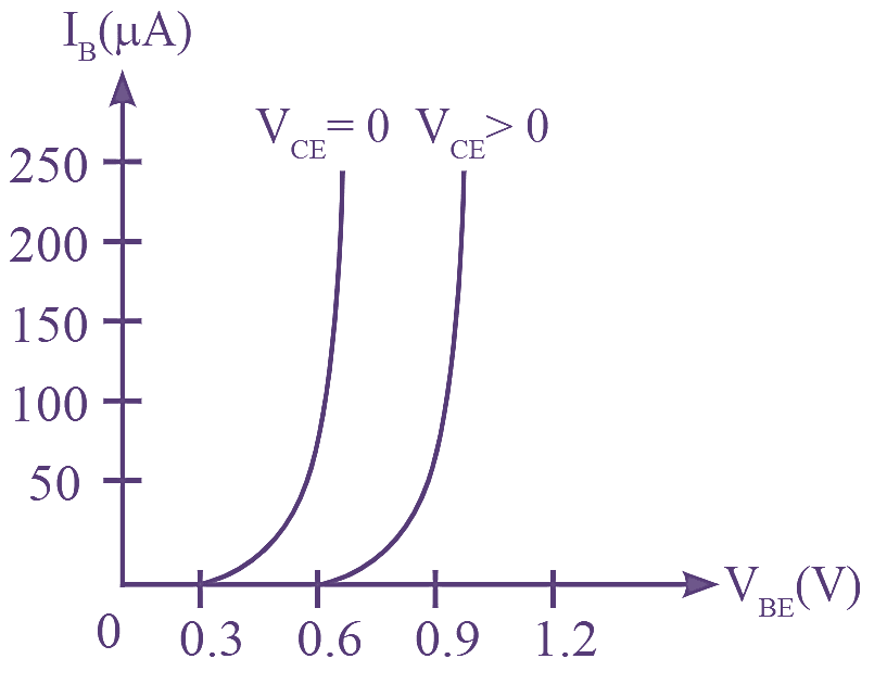
Figure 3: Input characteristics of CE transistor Configuration.
The curve plotted between base current IB and base-emitter voltage VBE keeping collector-emitter voltage VCE constant, gives the input characteristics of CE configuration.
The input characteristics of transistor in common-emitter configuration is as shown in figure (2).
It can be observed from figure (3), that input characteristics of CE transistor are drawn by taking VBE along the x-axis and IB along the y-axis.
The input characteristics of CE transistor are similar to the forward characteristics of a PN junction diode (i.e., for increase in VBE value, IB also increases gradually). Therefore, a higher order of resistance is observed at its input.
At constant VCE the ratio of change in base-emitter voltage ΔVBE to change in base current ΔIB gives the input resistance of CE transistor.
\[{{r}_{i}}={{\left. \frac{\Delta {{V}_{BE}}}{\Delta {{I}_{B}}} \right|}_{{{V}_{CE}}=\text{ Constent}}}\]
Output Characteristics
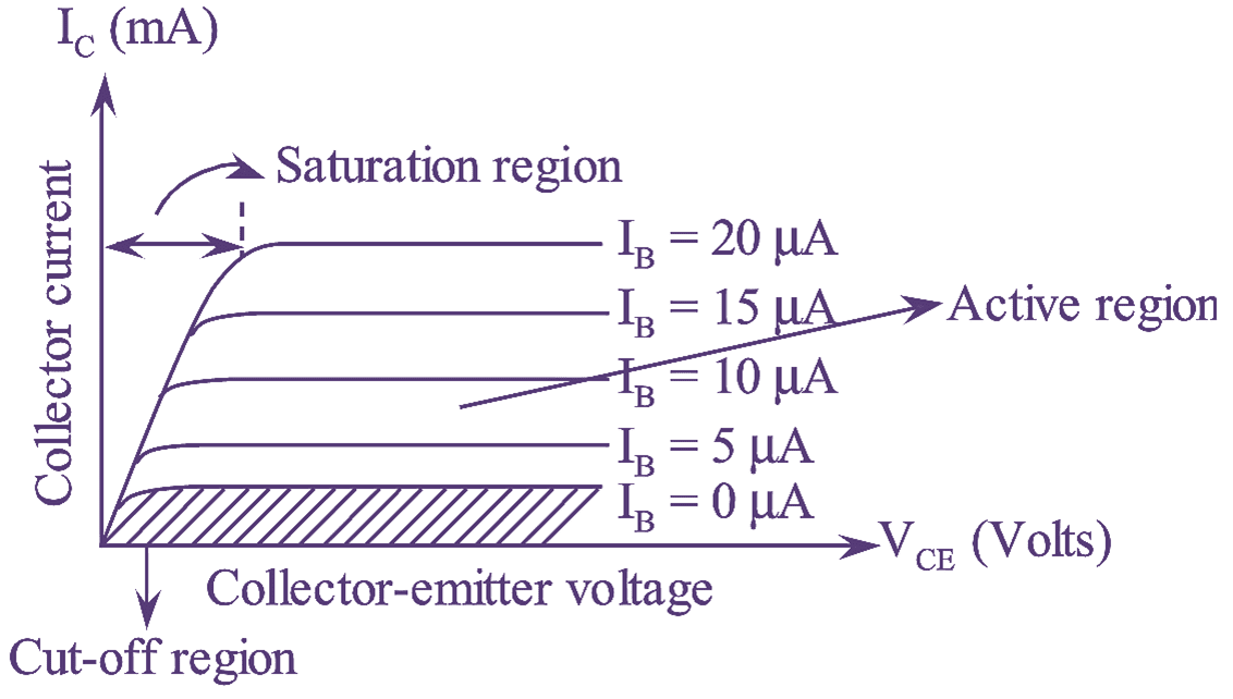
Figure 4: Output characteristics of CE transistor Configuration.
The curve plotted between collector current ‘IC‘ and collector-emitter voltage ‘VCE‘ , keeping base current ‘IB‘ constant gives the output characteristics of CE configuration. The output characteristics of transistor in common emitter configuration is as shown in figure (4). It can be observed from figure (4), that output characteristics of CE transistor are drawn by taking VCE along the x-axis and IC along the y-axis.
The collector current ‘IC‘ varies only for low values of VCE (i.e., between 0 and 1V), after which it becomes constant. The value of voltage till which IC depends on VCE is referred to as ‘knee voltage’. The CE transistor operates only in the region above knee voltage.
A small increase in IC with increasing VCE after the knee voltage, is only due to wider collector depletion layer. When VCE exceeds the knee voltage, then, IC ≈ βIB
At constant IB the ratio of change in collector-emitter voltage ‘ VCE‘ to the change in collector current IC gives the output resistance of CE transistor.
\[{{r}_{o}}={{\left. \frac{\Delta {{V}_{CE}}}{\Delta {{I}_{C}}} \right|}_{{{I}_{B}}=\text{ Constent}}}\]
Output Current:
When a transistor is operated in active region, its emitter is forward biased and collector is reverse biased. The collector current, IC is influenced by the emitter current (IE) and collector voltage (VC). This can be observed in the general expression of IC given by,
\[{{I}_{C}}=-\alpha {{I}_{E}}+{{I}_{CBO}}\left( 1-\exp \frac{{{V}_{c}}}{{{V}_{T}}} \right)…(1)\]
Where,
α = Large signal current gain
For, VC = Negative values of and |VC| >> VT
\[{{I}_{C}}=-\alpha {{I}_{E}}+{{I}_{CBO}}…(2)\]
For low values of VC or VCB, IC becomes independent of VC i.e., collector current (IC) is equal to α times the emitter current (IE).
Due to the opposite directions of lC and IE.
\[{{I}_{E}}=-({{I}_{C}}+{{I}_{B}})\]
Substituting ‘IE‘ in equation (2),
\[{{I}_{C}}=-\alpha (-({{I}_{C}}+{{I}_{B}})+{{I}_{CBO}}\]
\[=\alpha ({{I}_{C}}+{{I}_{B}})+{{I}_{CBO}}\]
\[{{I}_{C}}=\alpha {{I}_{C}}+\alpha {{I}_{B}}+{{I}_{CBO}}\]
\[{{I}_{C}}-\alpha {{I}_{C}}=\alpha {{I}_{B}}+{{I}_{CBO}}\]
\[(1-\alpha ){{I}_{C}}=\alpha {{I}_{B}}+{{I}_{CBO}}\]
\[{{I}_{C}}=\frac{\alpha }{1-\alpha }{{I}_{B}}+\frac{1}{1-\alpha }{{I}_{CBO}}\]
Since,
\[\beta =\frac{\alpha }{1-\alpha }\] And \[\alpha =\frac{\beta }{1+\beta }\]
\[1-\alpha =1-\frac{\beta }{1+\beta }\]
\[=\frac{1+\beta -\beta }{1+\beta }=\frac{1}{1+\beta }\]
Thus,
\[{{I}_{C}}=\beta {{I}_{B}}+(1+\beta ){{I}_{CBO}}\]