A unijunction transistor is a three-terminal device similar to a bipolar transistor but it has some unique characteristics that are quite different than ordinary PNP, NPN or field effect transistors. These characteristics make the UJT suitable in switching applications.
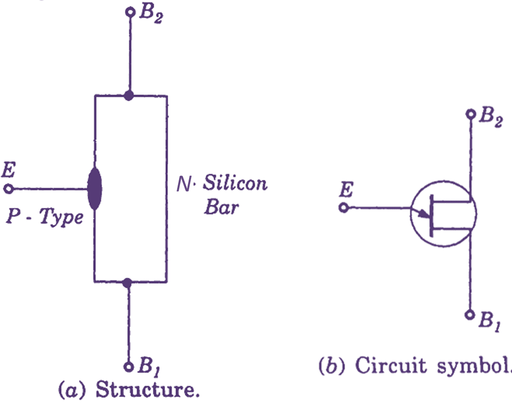
Figure 1: Unijunction Transistor (UJT).
A UJT can be conveniently considered as a bar or strip of high resistivity N-type silicon commonly called the base. Two contacts B1 and B2 are attached to it at opposite ends. A thin aluminum wire is alloyed at the middle of base to form a NP rectifying junction as shown in Fig. 1 (a). The connection brought from the aluminum P region is called the emitter. Fig. 1 (b) gives the circuit symbol of a unijunction transistor.
The construction of a UJT is similar to that of a JFET. The principal difference between the two is that the JFET has a much larger junction area compared to the UJT. Also, while the UJT is operated with the forward bias emitter junction, the JFET is always operated with gate-source junction reversed biased.
Unijunction Transistor (UJT) Characteristics
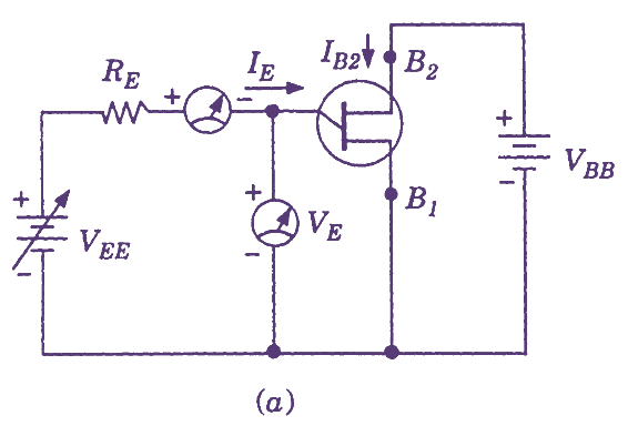
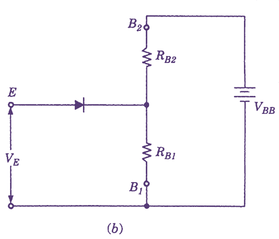
- Fig. 2. UJT characteristic : (a) Experimental setup for drawing (b) equivalent circuit of a UJT.
When DC voltage is connected between base 2 and base 1, as shown in Fig. 2 (a), the N-type bar behaves as a resistance and a current flows between base 2 and base 1 such that
\[{{I}_{B2}}= & \frac{{{V}_{BB}}}{{{R}_{B2}}+{{R}_{B1}}}\]
Where RB2 is the resistance of the bar measured between the junction and the terminal B2 and RB1 is the resistance offered by the region extending between junction and B1 as shown in Fig. 2 (b).
Due to this current flow, there is a uniform voltage distribution between the points B1 and B2. This potential distribution raises the potential of the mid-region of the bar with respect to the lower point B1 which is at zero potential. In this situation, if the emitter point is connected to ground (i.e. its potential VEE is made zero), then the potential of the N-region adjoining the P-N junction will be positive with respect to the P-region and the P-N junction is reverse biased. This potential cannot however be measured since meter load cannot be placed at the mid-region of the bar.
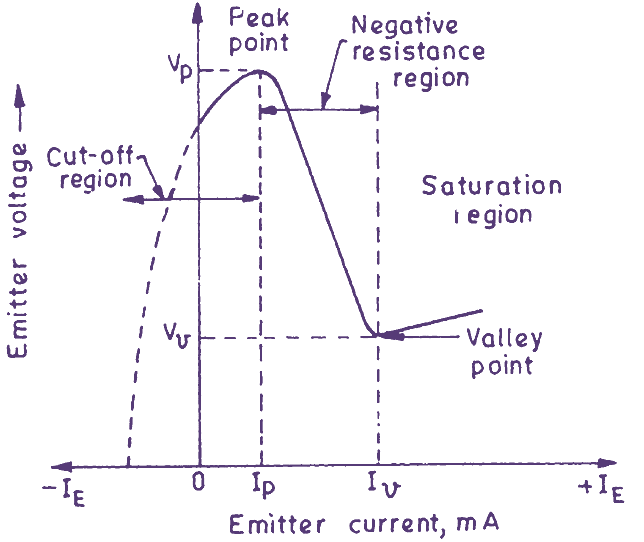
Fig. 3: Static characteristics of a UJT
Reverse biasing of the junction leads to a flow of reverse leakage current in the emitter as shown by dotted line in the static characteristics of the devices in Fig. 3.
If a voltage VE is applied between emitter and base 1 as shown in Fig. 2 (a), the potential of the emitter will be raised and the reverse bias across the P-N junction which is the difference between voltages at the emitter and the mid-region of the bar is lowered. Lowering the reverse bias decreases the reverse leakage current. When the emitter potential VE equals the potential of the mid-region of the bar, reverse bias is completely neutralized and tie reverse leakage current becomes zero.
A further increase in the emitter voltage VE causes the junction to be forward biased. When the emitter voltage overcomes the potential barrier, the emitter current shows a sharp increase. This point is marked as the peak point in Fig. 3 and the emitter voltage and current corresponding to the peak point are called the peak voltage and peak current. The emitter current completes its path through the lower region of the bar.
Since the N-channel region is of high resistivity, it has a small number of free electrons whereas there are large numbers of holes in the P-region. Thus, most of the emitter current flow results due to movement of holes. These holes cross over the junction and move through the region RB1. The presence of large number of holes in the lower region of the bar reduces the resistance RB1 to a very low value. This results in a sharp increase in the emitter current, voltage drop across emitter resistance RE also increases and potential of the emitter falls. Thus we obtain a region of characteristic in which an increase of current flow is accompanied by a drop in the emitter potential. Such a region is called the negative resistance region and is shown in Fig. 3.
The negative resistance region continues till a minimum emitter potential is reached. This is termed as the valley point and is marked in Fig. 3. Beyond the valley point, an increase in current is accompanied by a corresponding increase in emitter voltage and is termed as saturation region. The region of characteristic to the left of the peak point is called the cut-off region. Important applications of UJTs use the negative resistance region of characteristic.