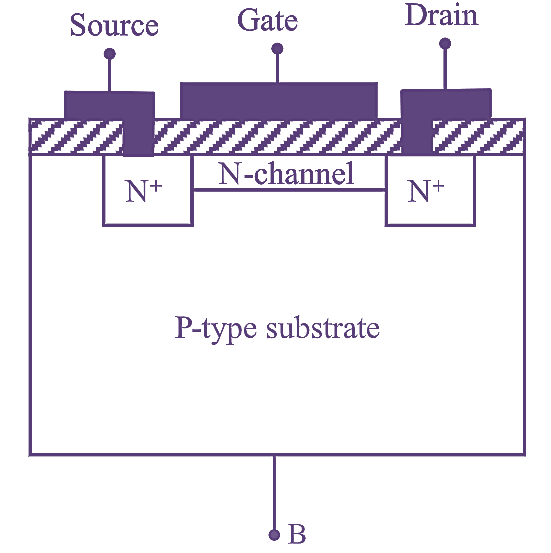
Figure 1: N-Channel Depletion MOSFET.
Construction of N-Channel Depletion MOSFET
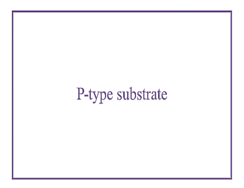
Figure 2.
The N-channel depletion MOSFET is constructed on a P-type silicon substrate as shown in figure (2). The substrate is a single crystal silicon wafer that provides physical support for the device.
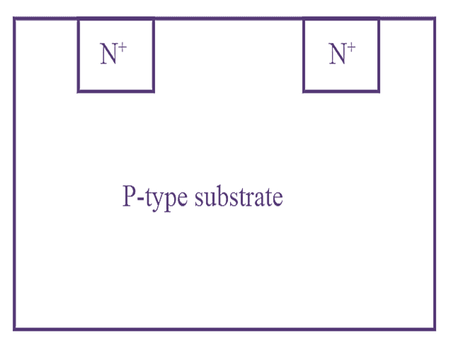
Figure 3.
Two heavily doped n-regions are diffused into the substrate as shown in figure (3). The n-regions are indicated as N+ in the figure. The two regions N+ act as source and drain for the MOSFET. Further, between the two N+ regions, that is, source and drain, an N-channel is implanted as shown in figure (3).
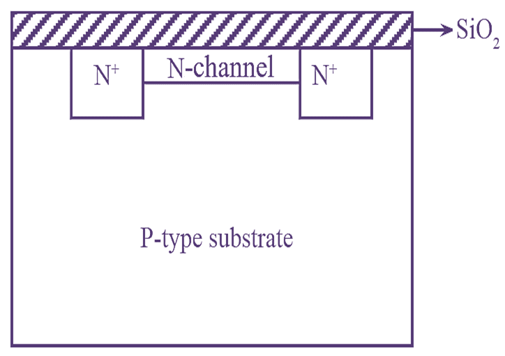
Figure 4.
A thin layer of silicon dioxide (SiO2) that is an electrical insulator grown on the surface of the substrate through oxidation process is shown in figure (4). The formation of metal and oxide layer creates a MOS capacitor. The metal of the gate and the semiconductor acts as plates of capacitor and the oxide layer acts as insulator of the MOS capacitor. Finally, metal is deposited on top of the oxide layer to form the gate electrode of the device. Metal contacts are also made to the source region, the drain region and the substrate. The device is packed and four terminals namely gate terminals (G), source terminals (S), drain terminals (D), and the substrate (also known as body) terminals (B) are taken out as shown in figure (1).
Working of N-Channel Depletion MOSFET
The principle of operation of MOSFET depends on the MOS capacitor. D-MOSFET requires the gate-source voltage, VGS to switch the device ‘OFF’. The operation of D-MOSFET is as follows,
Initially, when gate to source voltage VGS is equal to zero and a positive voltage is applied between drain and source, VDS then the charge carriers i.e., electrons in the N-channel are attracted by the positive terminals of the drain-to-source voltage. There is a flow of current through the N-channel between the two N+ regions. When gate-to-source voltage is made negative and a positive voltage is applied between drain and source, VDS, the electrons in the N-channel are repelled by the negative terminal of gate to source voltage and the holes which are majority carriers in p-substrate are attracted by the negative terminal of gate to source voltage. In the process, electrons moving away from the gate terminals recombine with holes moving towards the gate terminal. As a consequence, the total number of free electrons involving in the conduction of cm-rent are reduced. This in turn reduces the current ID flowing through the device. Finally, at VGS = VGS(off) ,ID becomes zero and the device operates same as JFET.
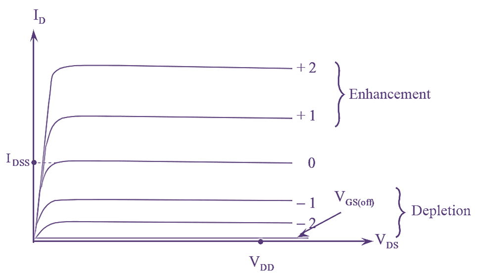
Figure 5: VI Characteristics of N-Channel Depletion MOSFET.
In contrast to the JFET, the D-MOSFET can be operated for positive value of gate to source voltage VGS. This is because of the insulation of gate terminal from the semiconductor body. Increase in the value of positive gate voltage increases the number of free electrons flowing through the channel. This in tum increases the current ID. The characteristics of D-MOSFET is shown in figure (5).