In this topic, you study the Principle of Step Down Chopper and its associated circuit diagram, Waveforms, Modes of operation, & theory.
The buck converter produces a lower average output voltage than the dc source input voltage.
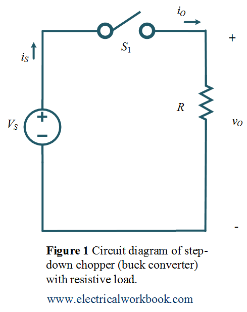
Circuit diagram of Buck Converter
The working of a buck regulator is explained using the circuit diagram as shown in Figure 1. The switch ${S_1}$ shown in the circuit diagram can be a conventional thyristor i.e., SCR, a GTO thyristor, a power transistor, or a MOSFET.
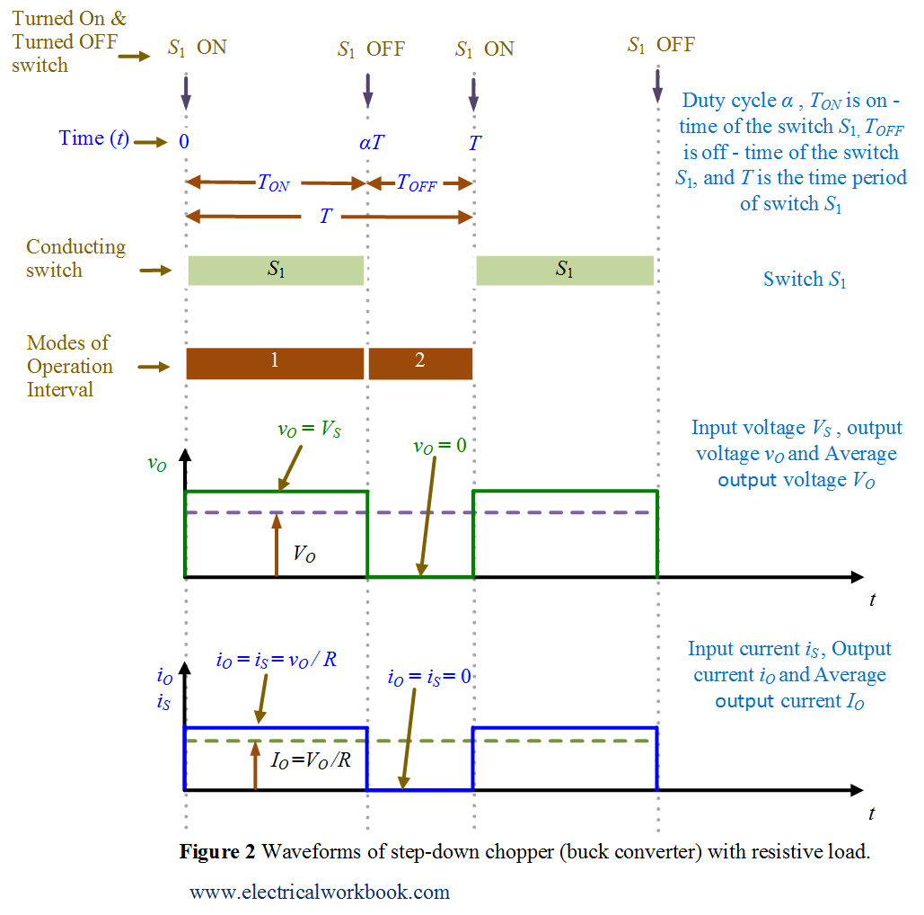
Waveforms of Buck Converter
The typical waveforms in the converter are shown in Figure 2.
Modes of Operation Interval of Buck Converter
The two modes in steady state operations are
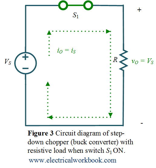
Mode of Operation Interval 1: –
The time interval is 0 ≤ t ≤ ${T_{ON}}$. The circuit diagram for Mode of Operation Interval 1 is shown in Figure 3 and the corresponding waveforms are shown in Figure 2. The switch ${S_1}$ is turned on and the resistive R load directly connects to input dc source voltage ${V_S}$ and hence ${v_O}$ = ${V_S}$, the source (or input) current flows through the Resistive load so ${i_S}$ = ${i_O}$ = ${v_O}/R$.
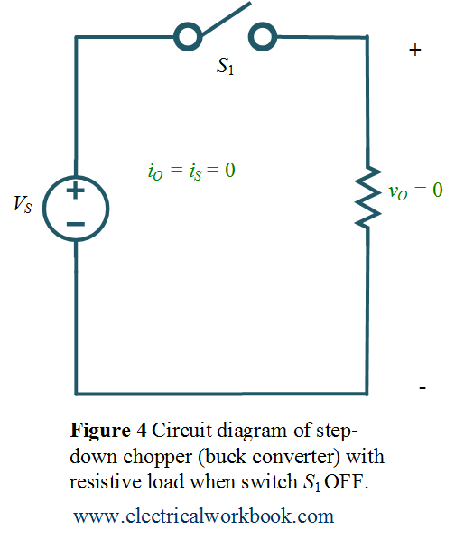
Mode of Operation Interval 2: –
The time interval is ${T_{ON}}$ ≤ t ≤ ${T_{OFF}}$. The circuit diagram for Mode of Operation Interval 2 is shown in Figure 4 and the corresponding waveforms are shown in Figure 2. The switch ${S_1}$ is turned off and the resistive R load disconnects from input dc source voltage ${V_S}$ and hence ${v_O}$ = 0, also the source (or input) current flows through the Resistive load will be ${i_S}$ = ${i_O}$ = 0.
Average output voltage ${V_O}$
Using the output voltage waveform as shown in Figure 2, the average value of the output voltage write as
\[{V_O} = \frac{{{T_{ON}}}}{{{T_{ON}} + {T_{OFF}}}}{V_S}…(1)\]
Also,
\[T = {T_{ON}} + {T_{OFF}}…(2)\]
Using Equation 1 and Equation 2 gives
\[{V_O} = \frac{{{T_{ON}}}}{T}{V_S} = \alpha {V_S}\]
So,
\[{V_O} = \alpha {V_S}…(3)\]
where,
$\alpha = {T_{ON}}/T$, $\alpha$ is the duty cycle of the chopper and the value of $\alpha$ lies between $0 ≤ \alpha ≤ 1$. ${T_{ON}}$ is the on – time of the switch ${S_1}$ or chopper , ${T_{OFF}}$ is the off – time of the switch ${S_1}$ or chopper, T is the chopping period, and the chopping frequency $f = 1/T$.
RMS output voltage ${V_{orms}}$
Using the output voltage waveform as shown in Figure 2, the RMS value of the output voltage write as
\[{V_{orms}} = {\left[ {\frac{{{T_{ON}}}}{{{T_{ON}} + {T_{OFF}}}}V_S^2} \right]^{1/2}}\]
or
\[{V_{orms}} = \sqrt \alpha \hspace{0.1cm} {V_S}\]