For the transistor to act as an amplifier is must be operated in its active region. The method of applying external voltages to operate the transistor in the active region is known as Transistor Biasing. For achieving a perfect amplification in amplifier circuit proper biasing is needed.
Types (or Methods) of Transistor Biasing
To accomplish this various biasing circuits are designed and the list of which is as follows,
- Fixed bias circuit
- Collector to base bias
- Potential divider bias.
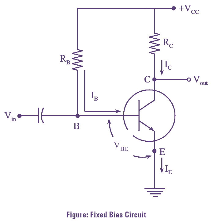
Fixed Bias Circuit
Fixed bias is also known as base resistor bias. In this, a common emitter amplifier is biased by connecting a resistor ‘RB‘ across the base and power supply terminals as shown in the figure below,
Applying KVL at the input side of the circuit in figure,
\[{{V}_{CC}}={{I}_{B}}{{R}_{B}}+{{V}_{BE}}…(1)\]
Rearranging equation (1),
\[{{I}_{B}}=\frac{{{V}_{CC}}-{{V}_{BE}}}{{{R}_{B}}}…(2)\]
The above equation is independent of IC.
Differentiating equation (2) with respect to IC,
\[\frac{d{{l}_{B}}}{d{{l}_{C}}}=0…(3)\]
The expression for stability factor ‘S’ for a CE configuration is,
\[S=\frac{1+\beta }{1-\beta \left( \frac{d{{l}_{B}}}{d{{l}_{C}}} \right)}…(4)\]
Using equation (3), equation (4) can be written as,
\[S=\frac{1+\beta }{1-\beta (0)}\] \[S=1+\beta \]
Since β is a large quantity, S is also very high. As a result, the circuit is very poor in stability. In practice, this circuit is not used for biasing the base.
Advantages of Fixed Bias Circuit
- The circuit is very simple.
- Number of components required are less.
Disadvantage Fixed Bias Circuit
- The circuit has very high value of stability factor S.
- Therefore it is highly unstable.
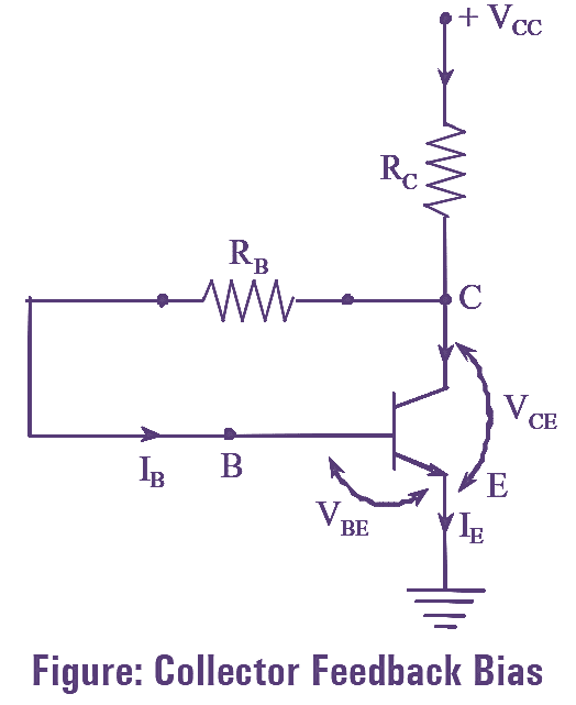
Collector to Base Bias
In this CE amplifier is biased by connecting a resistance ‘RB‘ across the collector and base terminals as shown in figure below. From the figure, it is clear that collector to base voltage forward biases the BE junction. Therefore sufficient base current flows through the base resistance ‘RB‘ and it causes zero signal collector current flowing in the circuit.
Applying KVL at the input side of circuit is shown in figure.
\[{{V}_{CC}}={{I}_{C}}{{R}_{C}}+{{I}_{B}}{{R}_{B}}+{{V}_{BE}}\]
And
\[{{I}_{C}}=\beta {{I}_{B}}\]
Then,
\[{{V}_{CC}}=\beta {{I}_{B}}{{R}_{C}}+{{I}_{B}}{{R}_{B}}+{{V}_{BE}}\]
\[{{I}_{B}}{{R}_{B}}={{V}_{CC}}-\beta {{I}_{B}}{{R}_{C}}-{{V}_{BE}}\]
\[{{R}_{B}}=\frac{{{V}_{CC}}-\beta {{I}_{B}}{{R}_{C}}-{{V}_{BE}}}{{{I}_{B}}}\]
Base resistance,
\[{{R}_{B}}=\frac{{{V}_{CC}}-\beta {{I}_{B}}{{R}_{C}}-{{V}_{BE}}}{{{I}_{B}}}\]
Alternatively,
\[{{V}_{CE}}={{V}_{BE}}+{{V}_{CB}}\]
\[{{R}_{B}}=\frac{{{V}_{CB}}}{{{I}_{B}}}=\frac{{{V}_{CE}}-{{V}_{BE}}}{{{I}_{B}}}\]
Thus,
\[{{R}_{B}} =\frac{{{V}_{CE}}-{{V}_{BE}}}{{{I}_{B}}}\]
Advantages of Collector to Base Bias Circuit
- It is easy and simple to design.
- It requires only ‘RB‘ for biasing.
Disadvantage Collector to Base Bias Circuit
- The circuit provides negative feedback that reduces the gain of an amplifier.
- Stability factor is fairly high.
Voltage Divider Bias (or) Self Bias
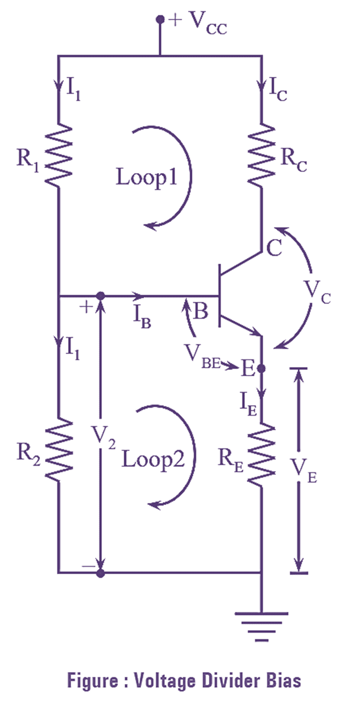
The most extensively used biasing circuit for maintaining stabilization is voltage divider bias circuit. It is as shown in figure. The circuit contains two resistors R1 and R2 connected to VCC in the base section of the transistor. The voltage drop across the resistor R2 forward biases the emitter base junction. The resistor RE connected to the emitter grants stabilization.
The current flowing through the resistance ‘R1‘ is I1. Since, the current flowing through the base is very small it can be assumed that the same current I1 flows through resistance by R2. Therefore I1 is given as,
\[{{I}_{1}}=\frac{{{V}_{CC}}}{{{R}_{1}}+{{R}_{2}}}\]
Further, since same current I1 is flowing through R1 and R2 it can be assumed that R1 and R2 are in series. Therefore, by using voltage division rule, the voltage drop across R2 is given as,
\[{{V}_{2}}=\left( \frac{{{R}_{2}}}{{{R}_{1}}+{{R}_{2}}} \right).{{V}_{CC}}…(4)\]
Apply KVL to the loop 2 shown in figure.
\[{{V}_{2}}={{V}_{BE}}+{{V}_{E}}\]
\[{{V}_{2}}={{V}_{BE}}+{{I}_{E}}{{R}_{E}}\]
\[{{I}_{E}}=\frac{{{V}_{2}}-{{V}_{BE}}}{{{R}_{E}}}\]
Thus,
\[{{I}_{E}}=\frac{{{V}_{2}}-{{V}_{BE}}}{{{R}_{E}}}\]
Generally for a CE configuration IE ≈ IC. Hence equation (4) can be written as,
\[{{I}_{C}}=\frac{{{V}_{2}}+{{V}_{BE}}}{{{R}_{E}}}…(5)\]
Where,
V2 – Voltage drop across ‘R2‘
VBE – Base emitter voltage.
Applying KVL to the output side of the circuit in figure,
\[{{V}_{CC}}={{I}_{C}}{{R}_{C}}+{{V}_{CE}}+{{V}_{E}}\]
\[{{V}_{CC}}={{I}_{C}}{{R}_{C}}+{{V}_{CE}}+{{I}_{E}}{{R}_{E}}\]
\[={{I}_{C}}({{R}_{C}}+{{R}_{E}})+{{V}_{CE}}\text{ (}{{I}_{C}}\approx {{I}_{E}}\text{)}\]
\[={{V}_{CE}}+{{I}_{C}}({{R}_{C}}+{{R}_{E}})\]
\[{{V}_{CE}}={{V}_{CC}}-{{I}_{C}}({{R}_{C}}+{{R}_{E}})\]
The circuit provides good stabilization through resistance ‘RE‘. It is explained using equation (5), that is,
\[{{V}_{2}}={{V}_{BE}}+{{I}_{C}}{{R}_{E}}\]
In the above expression, voltage V2 (across R2) is independent of IC and is given as,
\[{{V}_{2}}=\left( \frac{{{V}_{CC}}}{{{R}_{1}}+{{R}_{2}}} \right){{R}_{2}}\]
Since R1, R2 and VCC are constant, V2 is also constant. An increase in IC causes an increase in potential across RE (that is, ICRE). Since, V2 is constant an increase in ICRE must be compensated by a decrease in VBE Therefore, an increase in ICRE causes VBE to decrease and vice versa. In this manner the circuit provides good stabilization.
Advantages of Voltage Divider Bias Circuit
- It is most popular biasing circuit.
- Simple ‘RE‘ resistance provides good stability.
- Stability factor (S) in controlled by RE and Rth.
- Stability factor is small for this circuit compared to other techniques.