In this topic, you study Zener Diode Voltage Regulator – Circuit Diagram, Working & Derivation.
The zener is connected in parallel with the load, and hence it is called a zener diode voltage regulator. Fig. 1 shows the circuit of a zener diode shunt regulator.
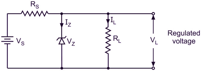
Fig. 1: Zener diode shunt regulator
The resistance RS is connected in series with the zener to limit the current in circuit and hence it is called as series current limiting resistor. The output voltage (VL) is taken across the load resistance (RL). The input voltage (VS) is set greater than zener voltage (VZ) for proper operation. The input current is given by,
\[{{\text{I}}_{\text{S}}}=\frac{{{\text{V}}_{\text{S}}}-{{\text{V}}_{\text{Z}}}}{{{\text{R}}_{\text{S}}}}\]
where,
VS = the d.c. input voltage to the regulator circuit
VZ = the zener voltage
If the resistance is negligible, then the load voltage is given by,
\[{{\text{V}}_{\text{L}}}=\text{ }{{\text{V}}_{\text{Z}}}\]
and current through the load resistance is given by,
\[{{\text{I}}_{\text{L}}}=\frac{{{\text{V}}_{\text{L}}}}{{{\text{R}}_{\text{L}}}}\]
The input current is the sum of zener current and load current i.e.
\[{{\text{I}}_{\text{S}}}=\text{ }{{\text{I}}_{\text{Z}}}+{{\text{I}}_{\text{L}}}\]
or
\[{{\text{I}}_{\text{Z}}}=\text{ }{{\text{I}}_{\text{S}}}-{{\text{I}}_{\text{L}}}\]
Working of zener diode shunt regulator
The working of zener diode voltage regulator is under two heads i.e. regulation with varying input voltage and regulation with varying load resistance.
Disadvantages of zener diode shunt regulator
The following are the disadvantages of a zener diode shunt regulator.
- The maximum load current is in mA.
- A large power dissipated in the zener diode and series resistance.