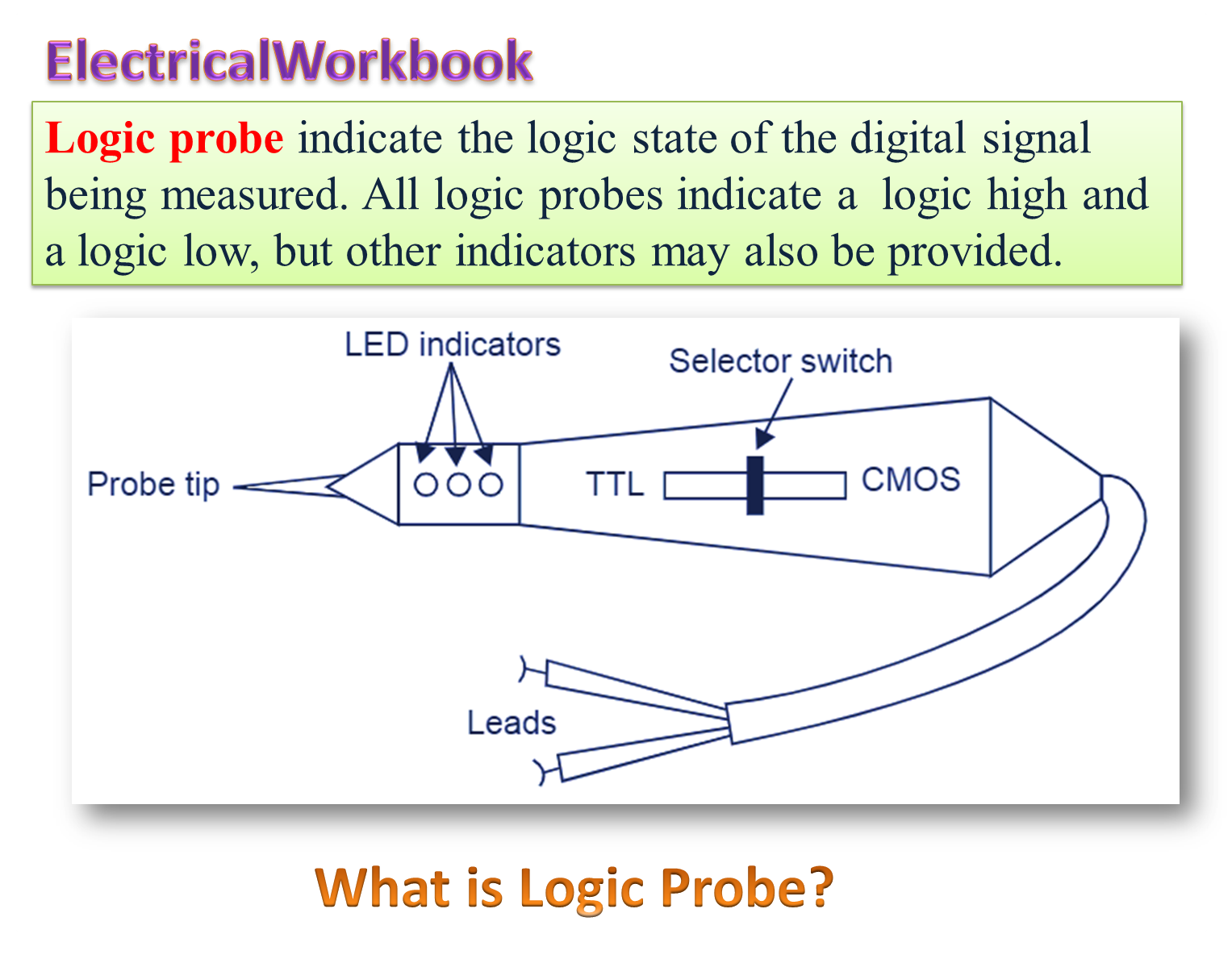
A logic probe is an equipment, which can indicate the logic state of a circuit, i. e., high logic (1) or low logic (0). A logic probe can view only one logic signal at a time and cannot store a record of the signal.
Block diagram of logic probe
The logic probe is powered by the circuit under test by connecting its leads to the DC supply lines of the board under test. Note that interconnection between two or more logic devices in a circuit is called a Node. The tip of the probe is placed in contact with the “node” under test. The selector switch is used to set for appropriate level of TTL (Transistor Transistor Logic) or CMOS (Complementary Metal Oxide Semi-conductor Logic). This setting can also be done automatically.
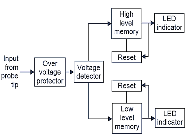
Fig. 1. Block diagram of logic probe.
Fig. 1. shows block diagram of the logic probe. The input logic level obtained from the probe tip is fed to a voltage detector through an over voltage protector. The voltage detector is set for appropriate voltage level for TTL or CMOS logics (manually or automatically). The detected voltage level say HIGH is fed to the appropriate memory (high) and the logic state is fed to the LED indicator till it is cleared by “reset” circuit. The process is repeated for LOW logic level. Recall that logic probe can detect one signal at a time.
Notes:
- Usually, the logic probe has 3 indicators: high logic, low logic, and pulse. The “Pulse” indicator flashes for pulsating output i.e., when transition takes place from one logic level to another.
- The logic probe can also detect the frequency pulses of shorter duration, which is difficult for a CRO.
- The logic probe can be used to detect faulty ICs and gates by observing one or zero outputs for all input combinations.