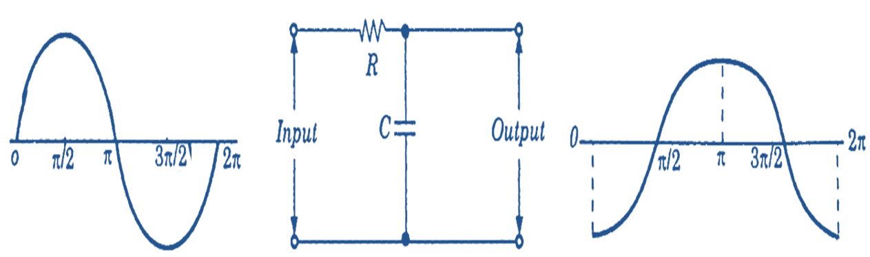
Figure 1: RC Integrator Circuit.
The RC integrator circuit contains a capacitor C and a resistor R, and their positions are shown in Fig. 1. Here the values of these elements are so arranged that the capacitive reactance offered at the operating signal frequency is very small in comparison to the value of the resistor so that the circuit current is approximately in phase to the input voltage. The voltage drop across the capacitor which is taken as the output lags the current by 90°. In other words, the output voltage will lag behind the input signal by 90°. The output waveform for a sinusoidal input is also shown in Fig. 1.
If the input voltage
\[{{v}_{i}}=V\sin \omega t\]
Since R >> XC
Then current
\[i\approx \frac{{{v}_{i}}}{R}=\frac{V\sin \omega t}{R}\]
Output voltage lags current by 90°
\[{{v}_{o}}={{v}_{c}}=\frac{V\sin \left( \omega t-{{90}^{\circ }} \right)}{R}=-\frac{V}{R}\cos \omega t ..(1)\]
Eq. (1) shows that the output (v0) is the integral of the input voltage. The above conclusion may also be reached mathematically.
We have output voltage
\[{{v}_{o}}={{v}_{c}}=\frac{Q}{C}\]
But we have
\[\frac{dQ}{dt}=i\]
Or
\[dQ=\,i.\text{ }dt\]
And
\[\text{Q = }\int{i.dt}\]
Thus
\[{{v}_{o}}=\frac{Q}{C}=\frac{1}{C}\int{i.dt}\]
But we know that
\[R>>{{X}_{C}}\]
And the current
\[i\approx \frac{{{v}_{i}}}{R}\]
\[{{v}_{o}}=\frac{1}{C}\int{\frac{{{v}_{i}}}{R}}.dt=\frac{1}{CR}\int\limits_{{}}^{{}}{{{v}_{i}}.dt} ..(2)\]
Eq 2 shows that the circuit output is the integral of the voltage
Working & Waveforms of RC Integrator
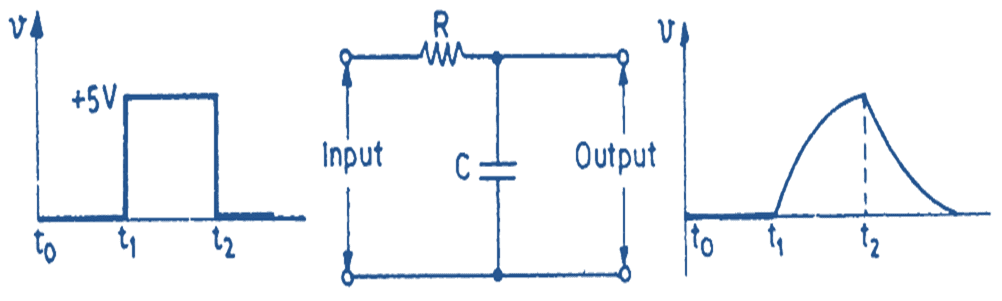
Fig. 2. Integrator output for a square wave input.
Now we feed a square wave input to the integrator and determine the shape of the output waveform. When the incoming square wave is zero between the time interval (t0 – t1), the output is also zero. At the instant t1, the input signal suddenly becomes +5 V, but since the capacitor C is uncharged the output voltage is zero. The output will show a rise only when the capacitor is charging.
For the time interval (t1 – t2), the input voltage remains +5 V and the capacitor continues to charge. The output voltage shows a rise as shown in the figure. The magnitude of the output voltage is dependent upon the charging current and the value of the capacitor. Since we have assumed resistor R to be very large, the charging takes place almost linearly as shown in the output waveshape.
At t2, the input voltage becomes zero and the input points are virtually shorted to ground. The capacitor, therefore, begins to discharge through R and the output falls as shown. After sometimes the output voltage, becomes zero.