Figure 1: RC Differentiator Circuit.
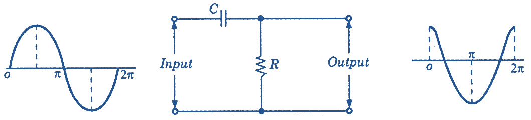
A simple RC differentiator circuit consists of a series combination of a capacitor C and a resistor R (see Figure 1). The input signal is fed across the combination and output is obtained across the resistor. Values of C and R are so selected that at the normal operating signal frequencies, the reactance of the capacitor is very large as compared to the resistor. Thus the current flowing in the differentiator circuit is to a large extent decided by the capacitive reactance; the current will be leading the input voltage by 90° approximately. Due to this current, the voltage developed across the resistor also leads the input voltage by 90°.
If the input is a sinusoidal signal and given by
\[{{v}_{i}}=V\sin \omega t\]
then the output voltage will be leading this voltage by 90°
\[{{v}_{o}}=V\sin \left( \omega t+{{90}^{{}^\circ }} \right)=V\cos \omega t\]
Thus, we find that the output is a differentiated form of the input signal. This can be proved mathematically.
The output voltage,
\[{{V}_{o}}=i.R\]
But since XC >> R, the current (i) is dependent upon capacitor alone. Therefore, the rate of change of charge across the capacitor gives the current
\[i=\frac{dQ}{dt} …(1)\]
but the charge Q across the capacitor C is given as
\[Q=C.\text{ }{{V}_{C}}\]
Where VC is the voltage across the capacitor.
As XC >> R, voltage across the capacitor is approximately same as vi i.e. VC ≈ vi Substituting this value in Eq. (1),
\[i=\frac{dQ}{dt}=\frac{d}{dt}\left( C.{{V}_{C}} \right)=C.\frac{d\left( {{v}_{i}} \right)}{dt}\]
And
\[{{v}_{0}}=i.R=CR.\frac{d\left( {{v}_{i}} \right)}{dt} …(2)\]
Eq. (2) shows that the output voltage is the differential coefficient of the input signal.
Working & Waveforms of RC Differentiator
Let us now feed a square wave signal at the input points and see how the output changes.
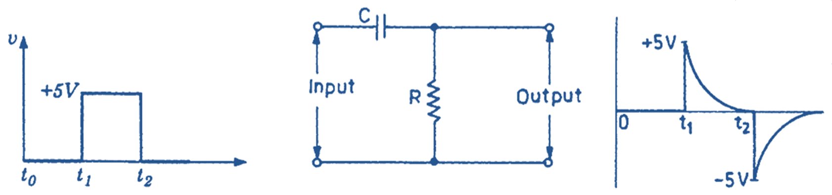
Fig. 2. RC Differentiator output for a square wave input.
When the input signal is zero between the duration (t0 – t1), there is no current flow in the differentiator circuit and the output voltage is zero. At t1, the input voltage suddenly rises to +5 V. Since the capacitor is uncharged, it acts as short circuit and allows maximum current. Thus full voltage appears across the resistor and zero voltage across capacitor.
During the interval (t1 – t2), the input voltage remains at +5 V. Thus, the capacitor begins to charge. As the voltage across the capacitor goes on building up, voltage across R goes on reducing. When capacitor is charged to the maximum voltage (+5V), the voltage across R becomes zero as shown in the output waveform.
At the instant t2, the input suddenly becomes zero and we get a situation where both the input points are at ground potential, i.e. (shorted). Thus the voltage across the capacitor appears across R with positive capacitor plate connected to ground end. Thus we get a negative output as shown in figure 2. The capacitor now discharges through the resistor R and the output voltage falls slowly to zero.