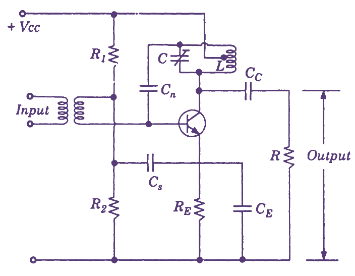
Single Tuned Amplifier circuits employ a single resonant circuit in the collector of the amplifier. The signal input is usually given to the amplifier through an input transformer but may also be fed through R-C coupling.
(a)
(b)
Fig. 1. A single tuned voltage amplifier using (a) capacitive coupled and (b) transformer coupled output.
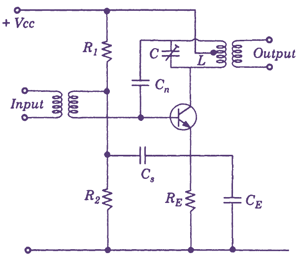
Similarly, the amplifier output may also be taken either through R-C coupling or by means of transformer coupling. The amplifier may employ a transistor, an FET or a vacuum pentode as the amplifying device. Fig. 10.8 shows different versions of a signal tuned voltage amplifier circuit with junction transistor as the amplifying device. An important thing to remember about the tuned voltage amplifiers is that they are small signal amplifiers and are, therefore, operated in class A. The necessary biasing is provided by R1, R2 and RE-CE combination in transistor circuits and RK-CK or RS-CS combination in FET circuits. Amplifier circuits employing vacuum tubes or FETs are also shown in Fig. 2.
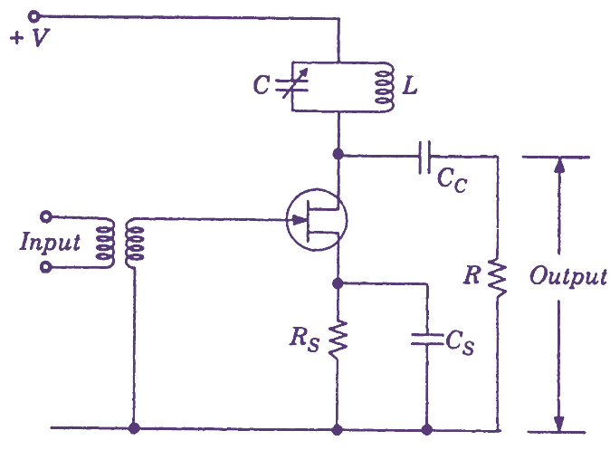
Fig. 2. Single-tuned voltage amplifier circuits using JFET.
Considering the transistor amplifier circuits of Fig. 1, the input signal available across the transformer secondary is given between base and emitter. One end of the secondary is joined directly to the transistor base while the other end is joined to the junction of R1 and R2. The capacitor CS connected between this junction and emitter acts as short circuit for the incoming signals allowing the signal to be applied between base and emitter. The DC potential present at the junction of R1-R2 is applied through the secondary winding of the transformer to the base. The FET amplifier circuit requires a negative bias for its operation and this is obtained from the self-biasing circuit connected at the source points. In this circuit, the transformer is connected between gate and ground.
The load in all these amplifier circuits is a parallel resonant circuit consisting of L and C which is designed to be resonant at the incoming signal frequency. In transistor amplifier circuit of Fig. 1, the junction capacitance between collector and base results in signal feedback from collector to base and this leads to complications like instability and reduction of the amplifier gain. To overcome this feedback, an equal but opposite signal is fed from collector to base through capacitor Cn. Signal of opposite polarity is obtained by tapping the coil L so that the signals present at the upper and lower end of the coil are 180° out of phase when measured with respect to the centre point which is at ground potential as far as signal is concerned. The signal present at the upper end is fed to the base through Cn. The output of the amplifier may be obtained by means of transformer or R-C coupling.
Frequency Response of Single Tuned Amplifier
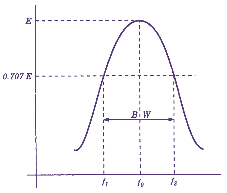
Fig. 3. Frequency response of a single-tuned amplifier.
The frequency response of single tuned amplifier circuits as given in Fig. 3 shows that the fall in gain when frequency deviates from the centre frequency f0, is not very sharp. Thus, even at frequencies that are slightly lower than f1 or slightly higher than f2 the gain is sufficiently large and these frequencies are not sharply discriminated. Thus, if the amplifier circuits corresponding to Fig. 1 or 2 are used, they will not only amplify the desired signal centred around f0. but will also pass signals having frequency close to f1 or f2 with sufficient amplifications. In other words, the amplifier does not completely reject the signals of adjacent channels or the adjacent channel rejection of the amplifier is not proper. This results in receiving an undesired signal along with a desired frequency signal. If the response of the tuned circuit is made sharp in order to reject the adjacent channels, then the bandwidth becomes very small and some frequencies of the desired signal are also rejected by the resonant circuit.